AI technical title is built by Patsnap AI team. It summarizes the technical point description of the patent document.
a light-emitting diode and gate-voltage technology, applied in the field of nanotube enabled, gate-voltage controlled light-emitting diodes, can solve the problems of low luminance efficiency, substantial source-drain current, and high drive voltage of lateral-type transistors using a standard fet structure, and achieve the effect of increasing the life of the devi
Active Publication Date: 2012-07-31
UNIV OF FLORIDA RES FOUNDATION INC
View PDF17 Cites 27 Cited by
Summary
Abstract
Description
Claims
Application Information
AI Technical Summary
This helps you quickly interpret patents by identifying the three key elements:
Problems solved by technology
Method used
Benefits of technology
Benefits of technology
[0007]Embodiments of the invention allow facile modulation of the electronic contact-barrier across the junction between single wall carbon nanotubes (SWNTs) and two distinct organic semiconductors. Specific embodiments relate to two devices: a vertical field effect transistor and a vertical light emitting transistor. The vertical architecture, which is readily facilitated by the specific properties of the nanotubes, allows the use of low mobility semiconductors that would otherwise be considered unsuitable for field effect transistors. For the light emitting transistor, the gate control permits new pixel drive schemes and increased device lifetimes.
Problems solved by technology
Lateral-type transistors using a standard FET structure require a high drive voltage due to factors such as a relatively long channel length, low luminance efficiency, and small aperture ratio.
This results in substantial source-drain current even when the gate field modulates the semiconducting nanotubes to minimize their conductance (the “off” state).
Unfortunately, the electronic mobilities of these compounds, which were initially about 5-6 orders of magnitude too low to be commercially useful, remain about an order of magnitude too low.
Such low mobility can be compensated for by bringing the source and drain electrodes closer together, reducing the semiconductor channel length (CL in FIG. 7A), but that greatly raises the cost of patterning the devices, removing much of the motivation.
While the optimized device exhibited ˜6 orders of magnitude current modulation, the low work function aluminum source electrode required an n-type active channel, restricting that device to the use of C60 as the channel material.
As forming a partly oxidized, ultra thin aluminum source electrode is difficult to produce commercially, constrains the choice of the organic active layers, and is susceptible to electromigration; hence, limiting the device lifetime other modes of forming an electrode that does not shield the gate field is desired.
Method used
Image
Click on the blue label to locate the original text in one second.
Reading with bidirectional positioning of images and text.
Examples
Embodiment Construction
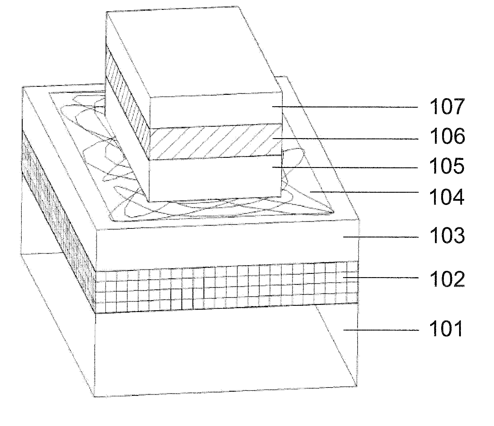
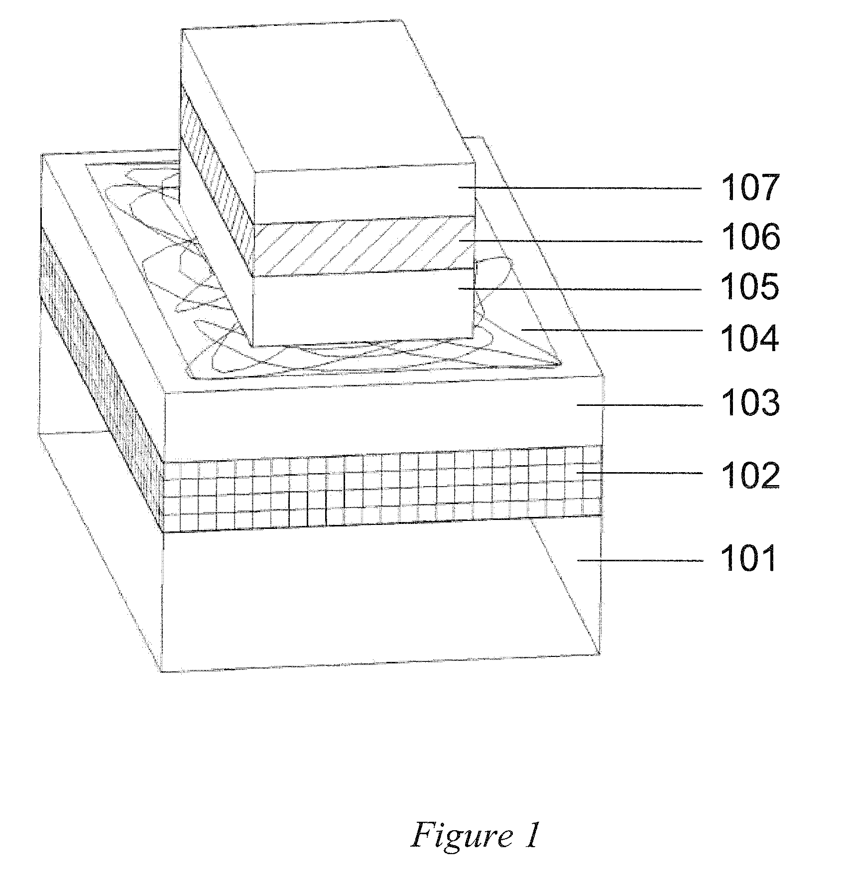
[0019]Embodiments of the invention are directed to light emitting transistors that have a gating electric field to control electronic transport between a first electrode comprising a dilute nanotube network and an electroluminescent semiconducting layer. The nanotube network includes open spaces that allow for penetration of the gate field into an electroluminescent layer. The gate field controls the current injection into the electroluminescent layer and thereby the visible light output from the device. Suitable applications of this technology include lighting, displays and signs, for example.
[0020]A gating electric field is used to modulate the barrier to electronic transport between a dilute nanotube network and a semiconducting layer by controlling current injection into the semiconducting layer. If the semiconducting layer is an electroluminescent material, the device becomes a gate-voltage controlled light emitting diode (GLED), also termed a light emitting transistor. FIG. 1 ...
PUM
Property
Measurement
Unit
gate voltage
aaaaa
aaaaa
gate voltage
aaaaa
aaaaa
gate voltages
aaaaa
aaaaa
Abstract
Embodiments of the invention relate to vertical field effect transistor that is a light emitting transistor. The light emitting transistor incorporates a gate electrode for providing a gate field, a first electrode comprising a dilute nanotube network for injecting a charge, a second electrode for injecting a complementary charge, and an electroluminescent semiconductor layer disposed intermediate the nanotube network and the electron injecting layer. The charge injection is modulated by the gate field. The holes and electrons, combine to form photons, thereby causing the electroluminescent semiconductor layer to emit visible light. In other embodiments of the invention a vertical field effect transistor that employs an electrode comprising a conductive material with a low density of states such that the transistors contact barrier modulation comprises barrier height lowering of the Schottky contact between the electrode with a low density of states and the adjacent semiconductor by a Fermi level shift.
Description
CROSS-REFERENCE TO RELATED APPLICATIONS[0001]This application is the U.S. national stage application of International Patent Application No. PCT / US2008 / 075866, filed Sep. 10, 2008, which claims the benefit of U.S. Provisional Application Ser. No. 60 / 971,147, filed Sep. 10, 2007, claims the benefit of U.S. Provisional Application Ser. No. 61 / 085,670, filed Aug. 1, 2008, and is a continuation-in-part of International Application No. PCT / US2007 / 072501, filed on Jun. 29, 2007, which claims the benefit of U.S. Provisional Application No. 60 / 817,521, filed on Jun. 29, 2006, all of which are hereby incorporated by reference herein in their entirety, including any figures, tables, or drawings.BACKGROUND OF THE INVENTION[0002]Light-emitting transistors combine the visible light emission properties of light emitting diodes (LEDs) with the switching properties of transistors. As driving elements, lateral- (e.g., field effect transistor (FET)) and vertical—(e.g., static induction transistor) ty...
Claims
Application Information
Patent Timeline
Application Date:The date an application was filed.
Publication Date:The date a patent or application was officially published.
First Publication Date:The earliest publication date of a patent with the same application number.
Issue Date:Publication date of the patent grant document.
PCT Entry Date:The Entry date of PCT National Phase.
Estimated Expiry Date:The statutory expiry date of a patent right according to the Patent Law, and it is the longest term of protection that the patent right can achieve without the termination of the patent right due to other reasons(Term extension factor has been taken into account ).
Invalid Date:Actual expiry date is based on effective date or publication date of legal transaction data of invalid patent.

