Liquid crystal display device, system and methods of compensating for delays of gate driving signals thereof

a display device and liquid crystal technology, applied in the direction of instruments, computing, electric digital data processing, etc., can solve the problems of horizontal lines or stripes visible on the left and right side, reducing the luminance of the corresponding pixel, and the visibility phenomenon of horizontal lines or stripes to be undetectable at the left and right margins of the display

Active Publication Date: 2012-07-31
SAMSUNG DISPLAY CO LTD
View PDF13 Cites 19 Cited by
  • Summary
  • Abstract
  • Description
  • Claims
  • Application Information

AI Technical Summary

Benefits of technology

[0010]In accordance with the disclosure, a liquid crystal display and a method of decreasing delay problems of a gate driving unit thereof are provided where each gate line is dually driven from both ends by providing gate driving circuit portions at both ends of each of the gate lines and where the synchronization delay problem between the gate driving and data line driving circuits is compensated for by feeding back a reset signal of the gate driving circuit.
[0025]The load signal generator calculates a delay time of the gate driving signal by dividing the number of gate lines provided on the display by a value of the clock count signal and responsively delays a falling timing point of the load signal corresponding to the calculated delay time of the gate driving signal and corresponding to the number rows scanned thus far when proceeding down one frame.
[0029]The load signal timing adjusting step includes calculating a delay time of the gate driving signal by dividing the number of gate lines provided with the gate driving signal by a value of the clock count signal and delaying a falling timing point of the load signal corresponding to the calculated delay time of the gate driving signal.

Problems solved by technology

Such a single driving system with split left and right portions sometimes has a problem in that artifacts in the form of left and right side horizontal lines or stripes become visible due to gate line propagation delays imposed on gate line activating pulses input form opposing sides of the display by the left and right drive portions.
The gate line delay may cause a pixel connected to a far end of a gate line to have insufficient time for charging to a desired pixel electrode voltage (corresponding to the data line voltage), thereby reducing luminance of the corresponding pixel.
In such a case, a luminance difference between two gate lines adjacent to each other is generated at the left or right sides of the neighboring gate lines, which causes the horizontal lines or stripes visibility phenomenon to undesirably appear at the left and right margins of the display.
So, there occurs a problem that a pixel connected to an Nth gate line located at a lower part of an LCD panel has a luminance lower than a luminance corresponding to the value of the data signal that is to be originally displayed because the open loop gate driving circuit is not perfectly synchronized with the timings of the data driving circuit and vise versa.
For instance, in case that a data signal of a green level (G) and a data signal of a blue level (B) are respectively provided by a data line driving unit in respective time slots associated with the data driving unit, if a gate driving signal is sequentially applied to a plurality of gate lines, there occurs a problem that the displayed luminance of the blue level (B) gets lower than what level of blue (B) was supposed to be originally displayed by a data signal representing the blue level (B) as one moves toward a lower part of an LCD panel.

Method used


Image

  • Liquid crystal display device, system and methods of compensating for delays of gate driving signals thereof
  • Liquid crystal display device, system and methods of compensating for delays of gate driving signals thereof
  • Liquid crystal display device, system and methods of compensating for delays of gate driving signals thereof

Examples


Embodiment Construction

[0041]Reference will now be made in detail to the embodiments illustrated in the accompanying drawings. Where practical, the same reference numbers will be used throughout the drawings to refer to same or like parts.

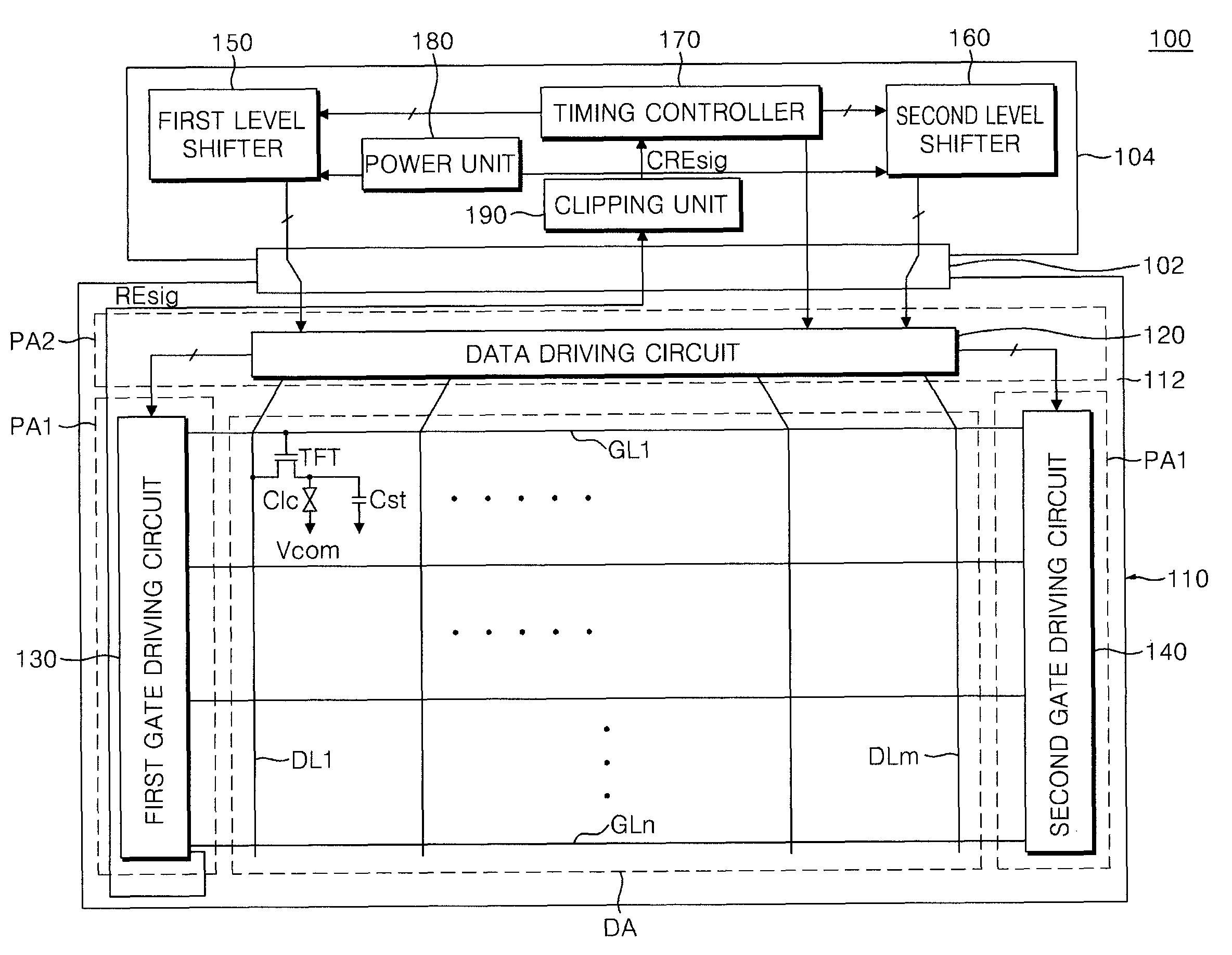
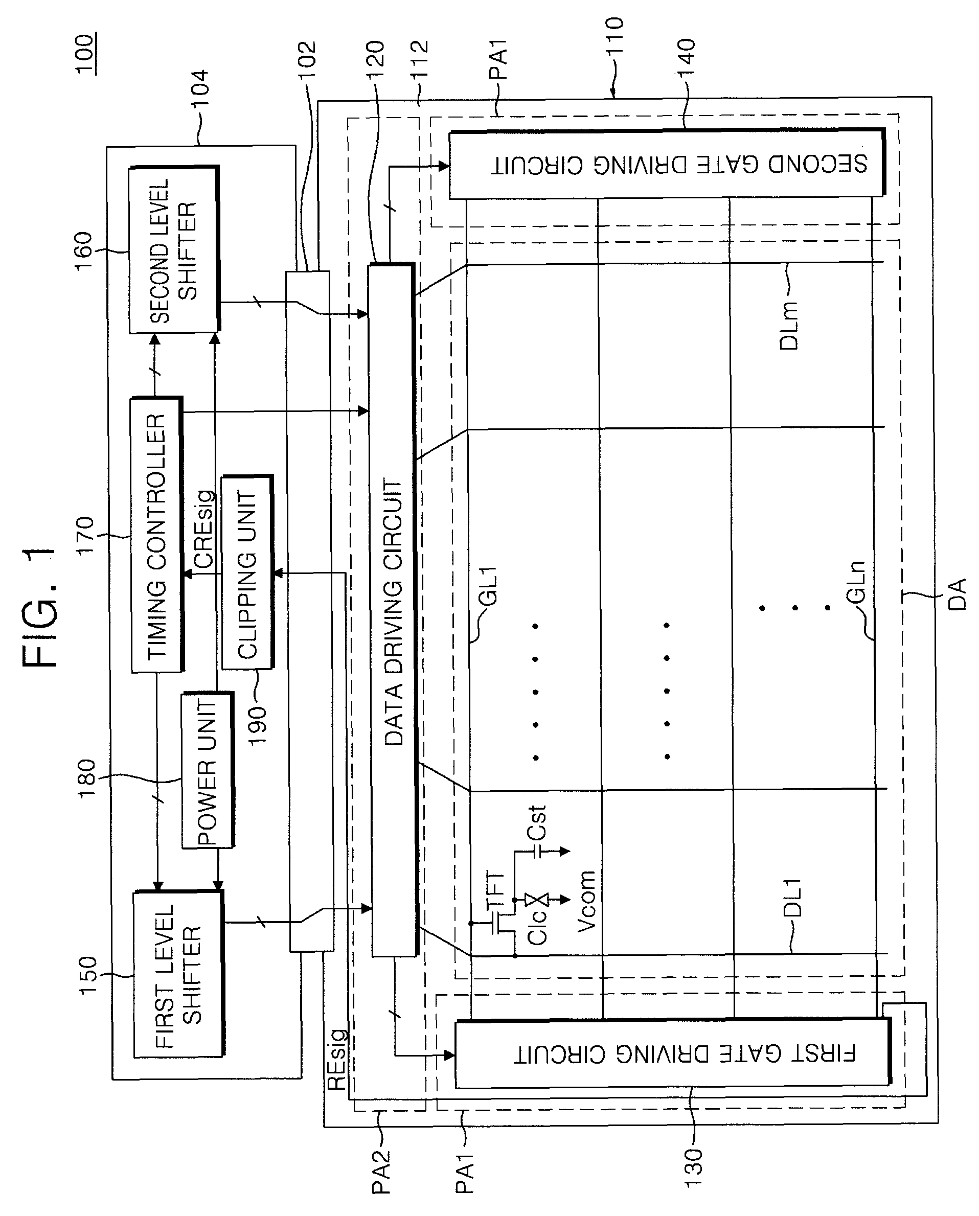
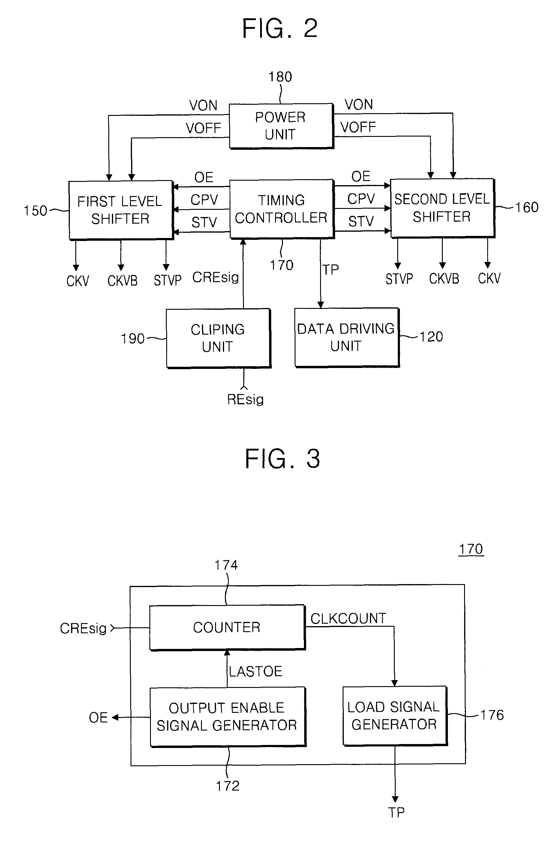
[0042]FIG. 1 is a block diagram of an LCD device 100 according to one embodiment. The LCD device 100 includes an LCD panel 110, a data driving circuit 120, a first gate driving circuit 130 on the left, a second gate driving circuit 140 on the right, a first level shifter 150 on the left, a second level shifter 160 on the right, a timing controller 170, a power supply unit 180, and a clipping unit 190.

[0043]The LCD panel 110 includes a TFT's-containing substrate 112, a color filters containing substrate (not shown), and a liquid crystal material (not shown) inserted between the TFTs substrate 112 and the color filters substrate.

[0044]The TFTs substrate 112 includes a display area DA, a first set of peripheral areas PA1, PA1′ (on the left and right sides), and a second per...


PUM


Abstract

A liquid crystal display device includes a gate driving shift register having symmetrically split circuit portions by which each of plural gate lines is dually driven from both ends of the gate line during ripple-through scanning of rows of the LCD device. The LCD device includes a timing controller generating an output enable signal and a gate clock, where the timing controller adjusts a timing of a load signal for deciding a data output timing point when data will be loaded into a currently activated display row. The data output timing point is a function of a delay measuring feedback signal that is used to measure the cumulative delays of the sequentially connected stages of the shift register.

Description

CROSS-REFERENCE TO RELATED APPLICATION[0001]This application claims priority to and benefit of Korean Patent Application No. 10-2006-0125334 filed in the Korean Intellectual Property Office on Dec. 11, 2006, the entire disclosure of which is incorporated herein by reference.FIELD OF INVENTION[0002]The present disclosure of invention relates to a liquid crystal display device, and more particularly, to a liquid crystal display (LCD) device that includes means for decreasing delays of pulsed gate driving signals thereof.DISCUSSION OF RELATED ART[0003]Generally, a liquid crystal display (“LCD”) device has an LCD panel for displaying a video image, a data driving unit for generating data-line signals of the LCD panel, and a gate driving unit for generating gate-line signals of the LCD panel. The LCD panel includes a plurality of gate lines, a plurality of intersecting data lines, and a plurality of pixels. Each of the pixels typically includes a thin film transistor (“TFT”) and a pair o...

Claims


Application Information

Patent Timeline
Patent Type & Authority Patents(United States)
IPC IPC(8): G09G3/36
CPCG09G3/3677G09G2310/0281G09G2310/0289G09G2310/08G09G2320/0223G09G2320/0233G02F1/133G09G3/20G09G3/36
Inventor YEO, JANG-HYUNKIM, WOO-CHULPARK, JAE-HYOUNG
Owner SAMSUNG DISPLAY CO LTD
Why Eureka
Try Eureka