Method for manufacturing organic electroluminescent device and organic electroluminescent device

a technology of electroluminescent devices and organic electroluminescent devices, which is applied in the manufacture of electrode systems, electric discharge tubes/lamps, and discharge tubes luminescent screens, etc., can solve the problems of difficult to reduce thickness variations, display failures, and new problems, and achieve high-quality images

Inactive Publication Date: 2012-08-07
SEIKO EPSON CORP
View PDF26 Cites 3 Cited by
  • Summary
  • Abstract
  • Description
  • Claims
  • Application Information

AI Technical Summary

Benefits of technology

[0012]An advantage of some aspects of the invention is that it provides a method for manufacturing an organic EL device which prevents the thickness variations of the organic functional layer so that the resulting organic EL device can display high-quality images. Another advantage of some aspects of the invention is that it provides an organic EL device manufactured by the method.

Problems solved by technology

However, such a process causes a new problem.
The thickness variations varies the amount of light emission, and thus leads to variations in brightness or color tone and results in display failure (inconsistencies in displayed images).
It is therefore difficult to reduce thickness variations resulting from the flow of the liquid composition.
However, the patent document does not propose any solution of the problem resulting from the stereoscopic shape of the base layer.
Furthermore, the region distant from the common partition wall is flat, and accordingly liquid composition applied to such a flat region is liable to flow.
If the distance from the common partition wall is increased to eliminate the negative effect of thickness variation in the vicinity of the common partition wall, the liquid composition becomes liable to flow and the risk of thickness variations is increased on the contrary.
Consequently, the thickness of the resulting functional layer formed is not easily varied among the effective pixels.
Accordingly, the thickness of the resulting functional layer is not easily varied due to the vapor condition of the solvent or the flow of the functional liquid.

Method used


Image

  • Method for manufacturing organic electroluminescent device and organic electroluminescent device
  • Method for manufacturing organic electroluminescent device and organic electroluminescent device
  • Method for manufacturing organic electroluminescent device and organic electroluminescent device

Examples


Embodiment Construction

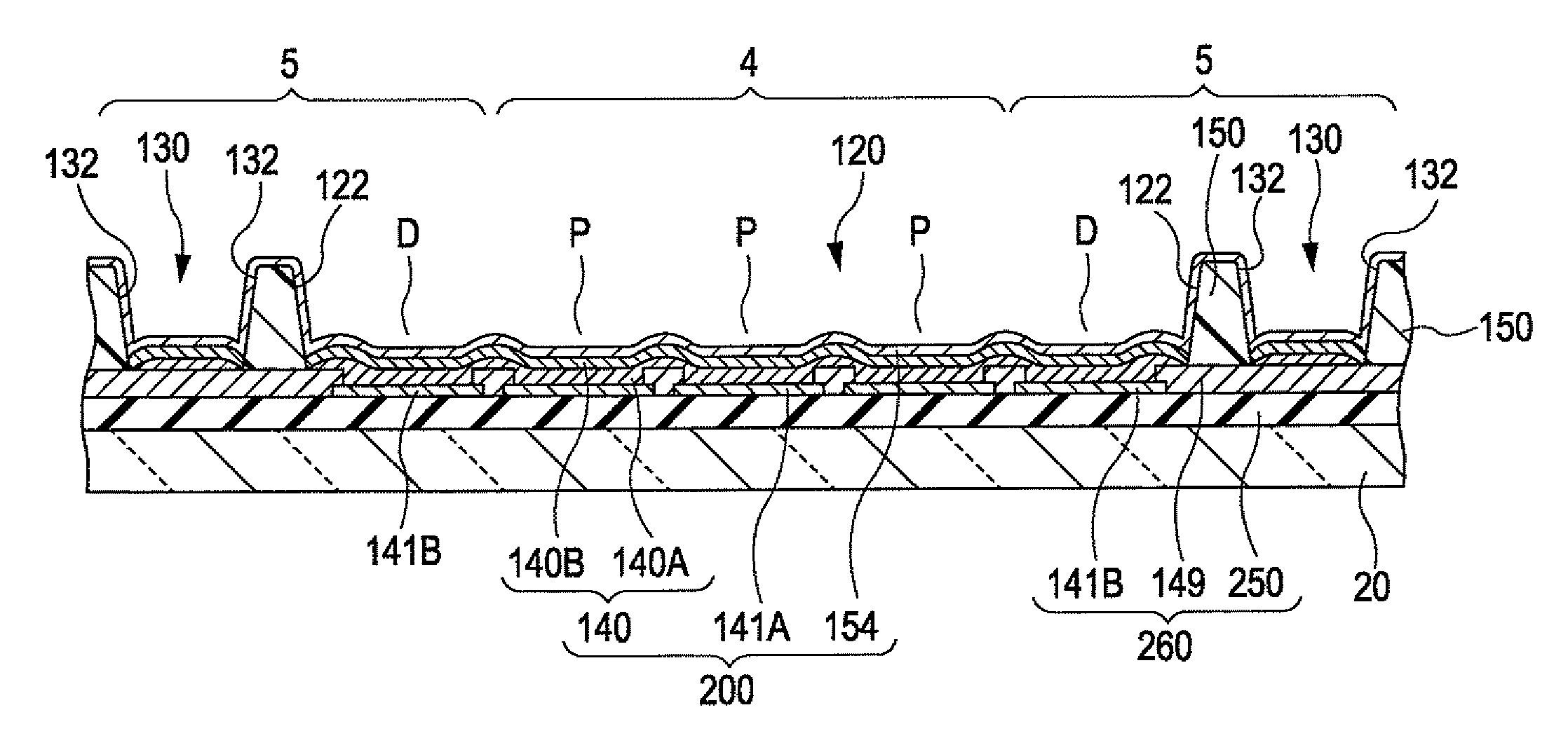
[0057]A method for manufacturing an organic EL device 1 according to an embodiment of the invention will now be described with reference to FIGS. 1 to 9. For the sake of visibility, the dimensional proportions and the numbers of parts may differ as needed in each figure.

[0058]Organic EL devices are classified into two types. One is a top emission type from which light emitted from organic EL elements is extracted through the substrate opposite to the substrate on which the organic EL elements are formed. The other is a bottom emission type from which the light is extracted through the substrate on which the organic EL elements are formed. The invention can be applied to either type to produce a favorable effect, and the following description does not limit the type of organic EL device except for some factors including material.

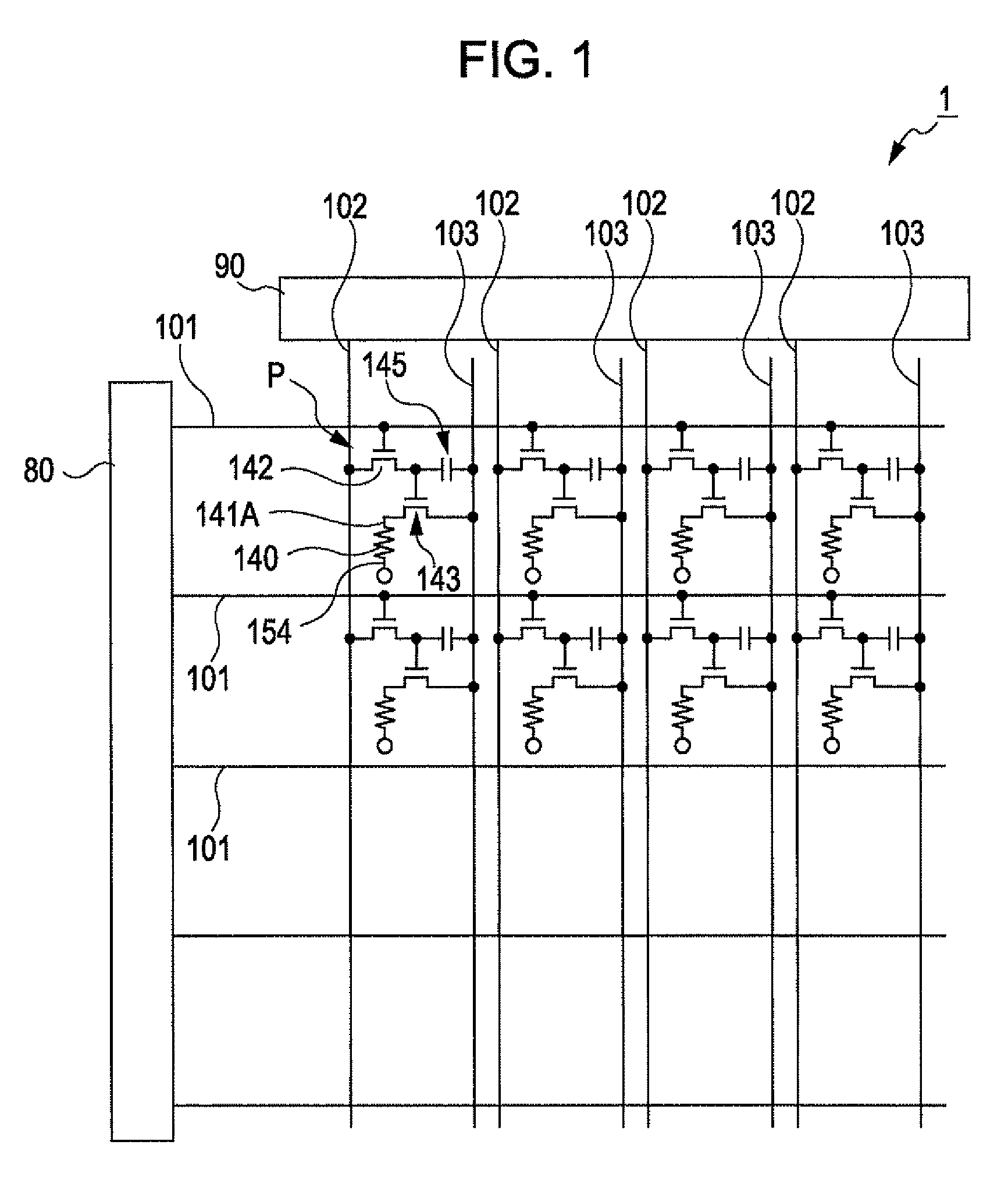
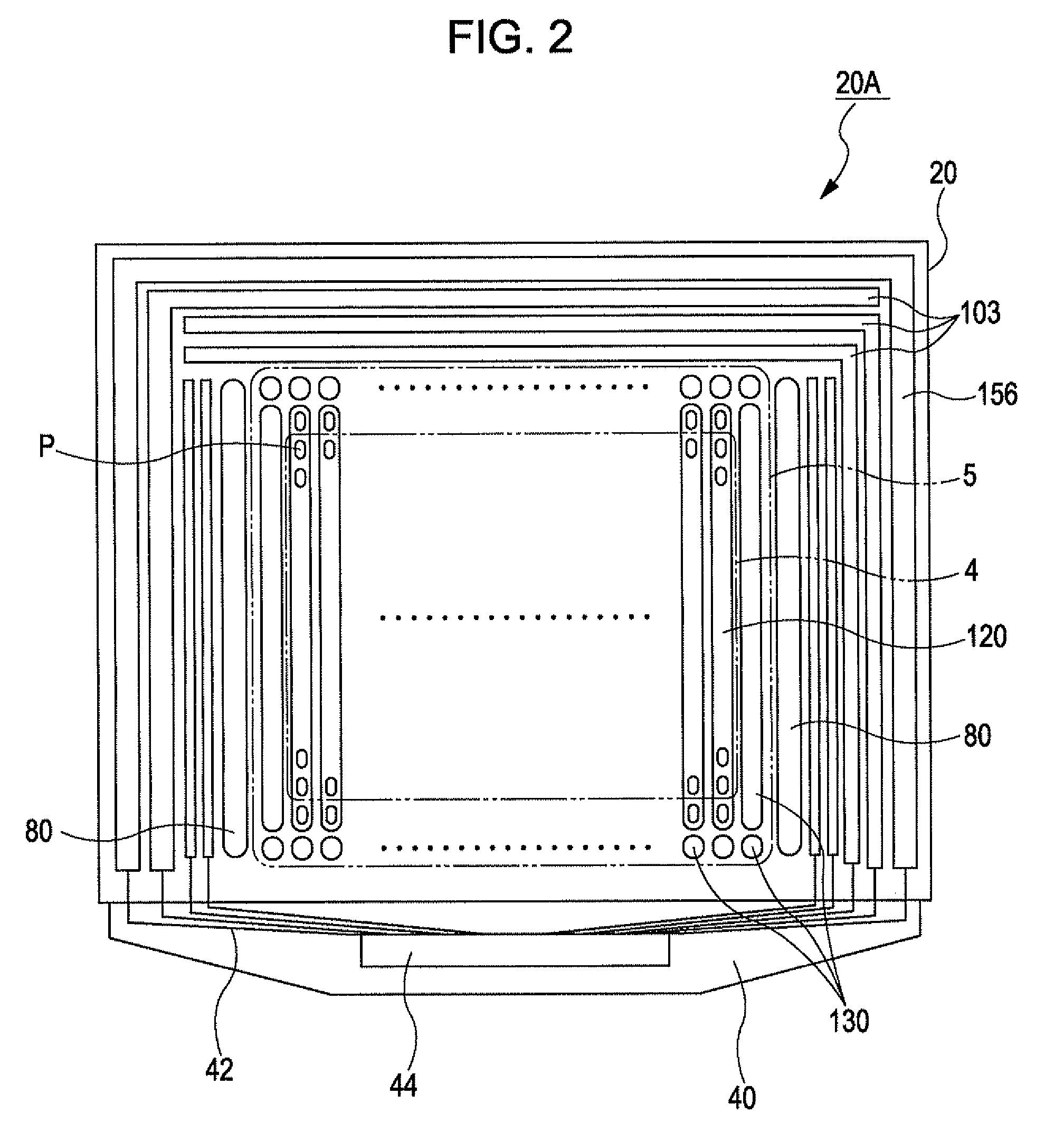
[0059]FIG. 1 is a schematic diagram of the wiring structure of the organic EL device 1 according to the present embodiment. The organic EL device 1 is of an ...


PUM


Abstract

An organic electroluminescent device includes partition walls dividing a region into a first region, a second region and a third region, a first organic layer disposed in the first region, a second organic layer disposed in the second region, and a third organic layer disposed in the third region. The first region includes a plurality of effective pixels involved in light emission, continuously disposed along a first aligning axis. Each effective pixel includes an effective pixel electrode, a common electrode, and the first organic layer between the effective pixel electrode and the common electrode. The second region and the third region oppose each other with the first region therebetween, and the first region, the second region and the third region are aligned along the first aligning axis.

Description

BACKGROUND[0001]1. Technical Field[0002]The present invention relates to a method for manufacturing an organic electroluminescent device and an organic electroluminescent device manufactured by the method.[0003]2. Related Art[0004]There has been developed, for example, electro-optic devices such as an organic EL display, optical writing heads such as a line head, and image-forming devices such as an optical printer, using organic electroluminescent (hereinafter referred to as organic EL) elements, which are a type of electro-optic element. An organic EL element generally has a structure including a luminescent layer made of an organic material between a pair of opposing electrodes. An organic EL device including such organic EL elements can display full color images by using red (R), green (G) and blue (B) color filters, or by using respective organic EL elements emitting those color lights.[0005]The organic EL element is formed by different methods depending on whether the luminesc...

Claims


Application Information

Patent Timeline
Patent Type & Authority Patents(United States)
IPC IPC(8): H05B33/00H01J9/00H05B33/10H01J1/62
CPCH01L27/3223H01L27/3244H01L27/3246H01L51/0005H01L2227/323H10K59/88H10K59/122H10K71/135H10K59/12H10K59/1201H01L2221/1089
Inventor TAKEI, SHUICHINIMURA, TORUUCHIDA, MASAHIRO
Owner SEIKO EPSON CORP
Why Eureka
Try Eureka