Demodulation circuit and RFID tag including the demodulation circuit

a demodulation circuit and circuit technology, applied in the field of demodulation circuits and rfid tags, can solve the problems of difficult to perform sufficient demodulation and insufficient rectifying functions, and achieve the effects of improving the ability of demodulation circuits, favorable data transmission and reception, and excellent characteristics

Active Publication Date: 2012-09-04
SEMICON ENERGY LAB CO LTD
View PDF150 Cites 10 Cited by
  • Summary
  • Abstract
  • Description
  • Claims
  • Application Information

AI Technical Summary

Benefits of technology

[0007]By the way, energy of electromagnetic waves is inversely proportional to the square of the distance between a point on which the electromagnetic waves are radiated and an observation point. That is, as the distance between a communication device and an RFID tag becomes longer, the energy of electromagnetic waves that the RFID tag receives becomes lower; on the contrary, as the distance between the communication device and the RFID tag becomes shorter, the energy of electromagnetic waves that the RFID tag receives becomes higher.
[0010]In the invention disclosed herein, a material which enables a reverse current to be small enough, for example an oxide semiconductor material, which is a wide bandgap semiconductor, is used in a transistor in a demodulation circuit, whose gate terminal and drain terminal (or source terminal) are connected to each other. By using a semiconductor material which enables a reverse current of a transistor whose gate terminal and drain terminal (or source terminal) are connected to each other to be small enough, even in the case where electromagnetic waves with large amplitude are received, a sufficient demodulation ability can be secured.
[0016]By using any of the embodiments of the demodulation circuit, an RFID tag having excellent characteristics can be obtained.
[0023]By using an oxide semiconductor in a transistor whose gate terminal and drain terminal (or source terminal) are connected to each other, a reverse current can be made small enough. Therefore, using this transistor, an ability of a demodulation circuit can be improved sufficiently. Accordingly, even when the distance between a communication device and an RFID tag is short, favorable data transmission and reception can be carried out.
[0024]In this manner, by using a transistor including an oxide semiconductor (in a broad sense, a transistor in which a reverse current can be small enough) in part of a demodulation circuit, the demodulation circuit can have excellent characteristics. Further, with the use of the demodulation circuit, an RFID tag having excellent characteristics can be realized.

Problems solved by technology

However, for example in an RFID tag provided with the demodulation circuit disclosed in Patent Document 1 which utilizes a rectifying function of a transistor whose gate terminal and drain terminal (or source terminal) are connected to each other, a reverse current is generated in the transistor when electromagnetic waves with large amplitude are received, so that a sufficient rectifying function cannot be obtained.
In other words, it is difficult to perform sufficient demodulation.

Method used


Image

  • Demodulation circuit and RFID tag including the demodulation circuit
  • Demodulation circuit and RFID tag including the demodulation circuit
  • Demodulation circuit and RFID tag including the demodulation circuit

Examples


embodiment 1

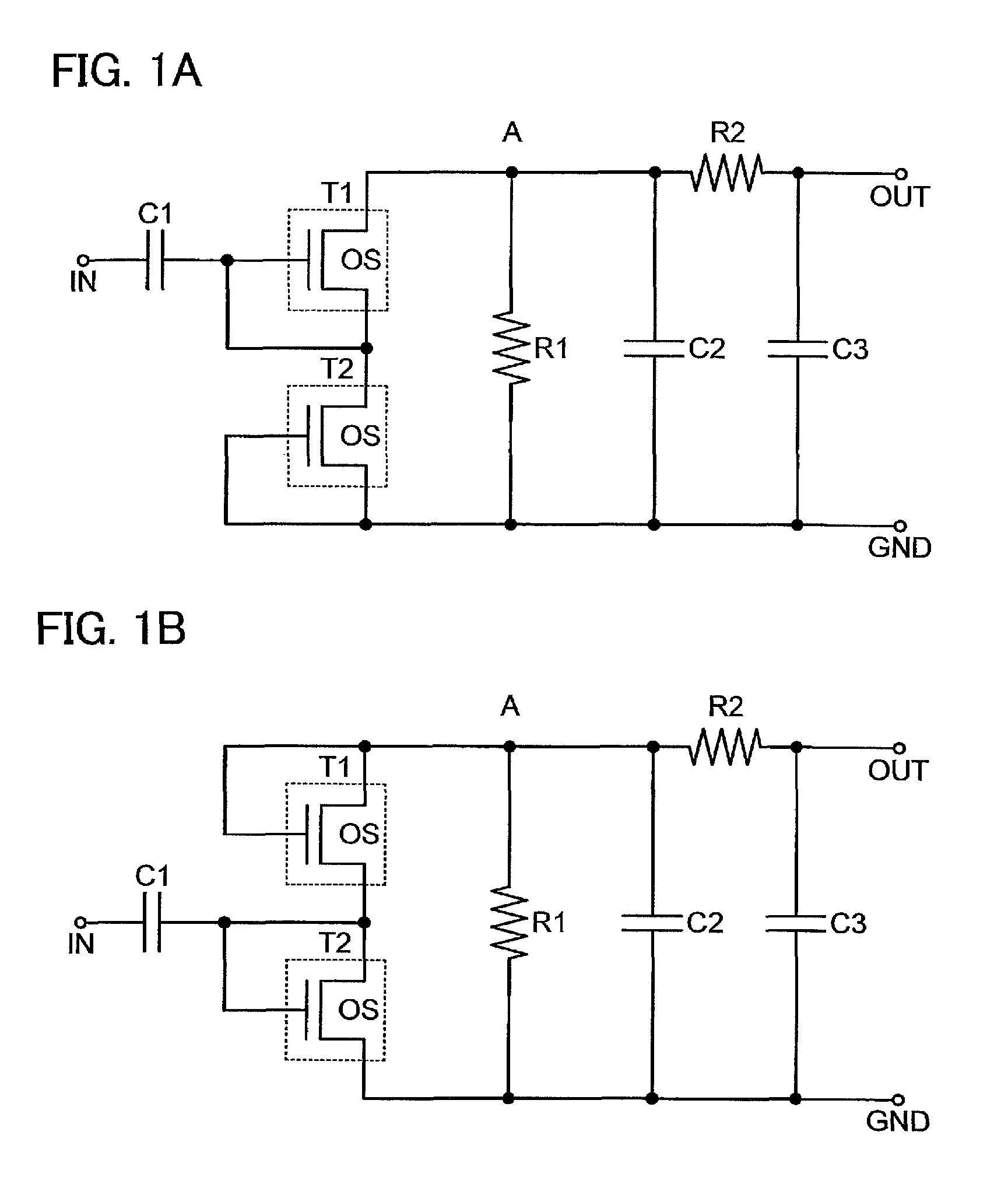
[0035]In this embodiment, a circuit configuration and the like of a semiconductor device according to an embodiment of the invention disclosed herein will be described with reference to FIGS. 1A and 1B, FIGS. 2A to 2C, and FIGS. 3A to 3C. Note that in circuit diagrams, “OS” may be written beside a transistor in order to indicate that the transistor includes an oxide semiconductor.

[0036]First, circuit configurations and functions of components of a semiconductor device of an embodiment of the invention disclosed herein will be described with reference to FIGS. 1A and 1B.

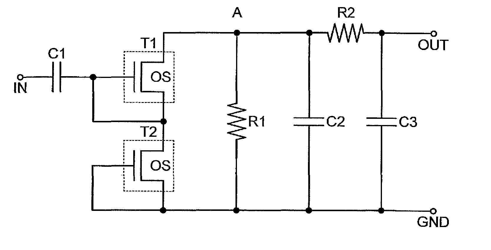
[0037]FIG. 1A shows an example of a demodulation circuit of the invention disclosed herein. The demodulation circuit includes a first transistor T1, a second transistor T2, a first capacitor C1, a second capacitor C2, a third capacitor C3, a first resistor R1, and a second resistor R2.

[0038]Here, a gate terminal of the first transistor T1, a drain terminal (or a source terminal) of the first transistor T1, a source te...

embodiment 2

[0058]In this embodiment, an RFID tag which is an example to which the demodulation circuit described in the above embodiment is applied will be described with reference to FIG. 4.

[0059]The RFID tag of this embodiment includes a memory circuit storing necessary data and exchanges data with the outside using contactless means such as wireless communication. Having these features, the RFID tag can be used for an individual authentication system in which an object is identified by reading individual information of the object, or the like. Note that the RFID tag is required to have extremely high reliability in order to be used for this purpose.

[0060]A configuration of the RFID tag will be described with reference to FIG. 4. FIG. 4 is a block diagram showing a configuration of an RFID tag.

[0061]As shown in FIG. 4, an RFID tag 300 includes an antenna 304 which receives a radio signal 303 that is transmitted from an antenna 302 connected to a communication device 301 (also referred to as ...

embodiment 3

[0069]In this embodiment, examples of a transistor which can be applied to the demodulation circuit described in the above embodiment will be described with reference to FIGS. 5A to 5D. There is no particular limitation on the structure of the transistor; for example, a staggered type or a planar type having a top-gate structure or a bottom-gate structure can be employed as appropriate. Further, the transistor may have any of a single gate structure including one channel formation region, a double gate structure including two channel formation regions, or a triple gate structure including three channel formation regions. Alternatively, the transistor may have a dual gate structure including two gate electrode layers positioned over and below a channel region with a gate insulating layer provided therebetween.

[0070]FIGS. 5A to 5D each illustrate an example of a cross-sectional structure of a transistor. Transistors illustrated in FIGS. 5A to 5D are transistors including an oxide semi...


PUM


Abstract

An object is to provide a demodulation circuit having a sufficient demodulation ability. Another object is to provide an RFID tag which uses a demodulation circuit having a sufficient demodulation ability. A material which enables a reverse current to be small enough, for example, an oxide semiconductor material, which is a wide bandgap semiconductor, is used in part of a transistor included in a demodulation circuit. By using the semiconductor material which enables a reverse current of a transistor to be small enough, a sufficient demodulation ability can be secured even when an electromagnetic wave having a high amplitude is received.

Description

TECHNICAL FIELD[0001]The invention disclosed herein relates to a demodulation circuit and an RFID tag that utilizes the demodulation circuit.BACKGROUND ART[0002]Recently, semiconductor devices that are capable of transmitting and receiving data without contact have been actively developed. Such semiconductor devices are particularly called RFID (radio frequency identification) tags, ID tags, IC tags, IC chips, RF tags, wireless tags, electronic tags, wireless chips, transponders, and the like.[0003]The data transfer between the RFID tag and a communication device is generally carried out in such a manner that a device on the transmission side (e.g., the communication device) transmits a modulated carrier wave, and the device on the reception side (e.g., the RFID tag) demodulates the modulated carrier wave.[0004]As one of the methods for modulating a carrier wave, there is an amplitude modulation method (an amplitude shift keying (ASK) modulation method). An ASK modulation method is ...

Claims


Application Information

Patent Timeline
Patent Type & Authority Patents(United States)
IPC IPC(8): H03D1/00
CPCH03D1/18H01L27/1225G06K19/07
Inventor MATSUZAKI, TAKANORISHIONOIRI, YUTAKA
Owner SEMICON ENERGY LAB CO LTD
Why Eureka
Try Eureka