
Liquid crystal display panel

a liquid crystal display panel and display panel technology, applied in non-linear optics, instruments, optics, etc., can solve the problems of light leakage severely affecting the display quality of the lcd panel, the misalignment between two substrates, and the generation of displacement. , to achieve the effect of limiting the displacement of the spacers and preventing the misalignmen

Active Publication Date: 2012-09-18
AU OPTRONICS CORP
View PDF4 Cites 0 Cited by
  • Summary
  • Abstract
  • Description
  • Claims
  • Application Information

AI Technical Summary

Benefits of technology

[0007]An aspect of the invention provides a liquid crystal display (LCD) panel capable of preventing an misalignment between two substrates by limiting a displacement of the spacers.
[0009]In summary, the position limiting structures of the LCD panel according to embodiments of the invention can limit the displacement of the spacers, so as to prevent an misalignment between two substrates when the LCD panel is pressed or under stress. Accordingly, a light leakage phenomenon of the LCD panel can be avoided, and thereby the LCD panel is able to achieve a preferable display quality.

Problems solved by technology

However, when the LCD panel is pressed or under stress, a relative displacement may be generated between the color filter substrate and the active device array substrate, such that a light originally shielded by the black matrix is leaked.
Therefore, when relative displacement is generated between the color filter substrate and the active device array substrate, light leakage severely affects a display quality of the LCD panel.

Method used


Image

  • Liquid crystal display panel
  • Liquid crystal display panel
  • Liquid crystal display panel

Examples


Embodiment Construction

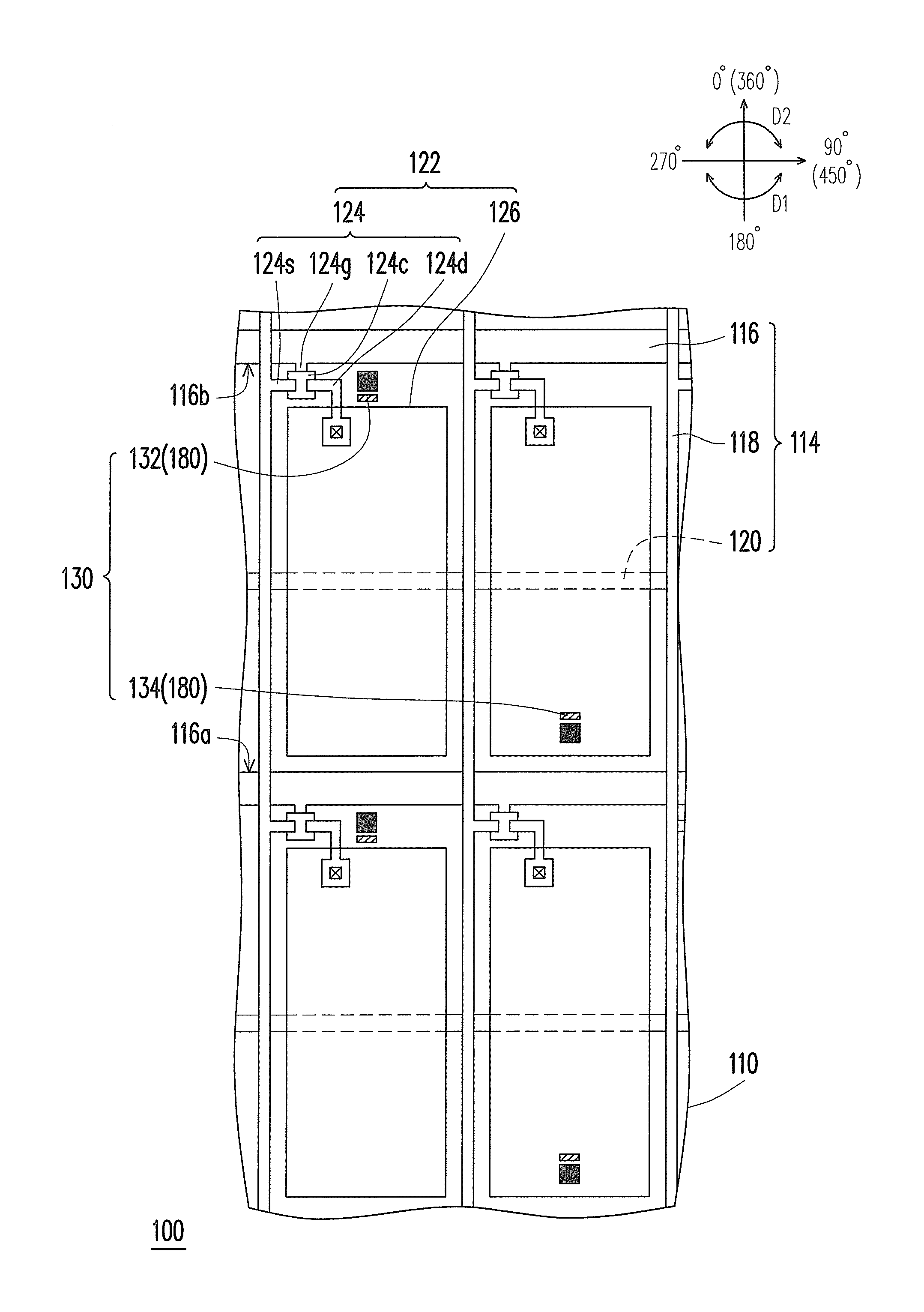
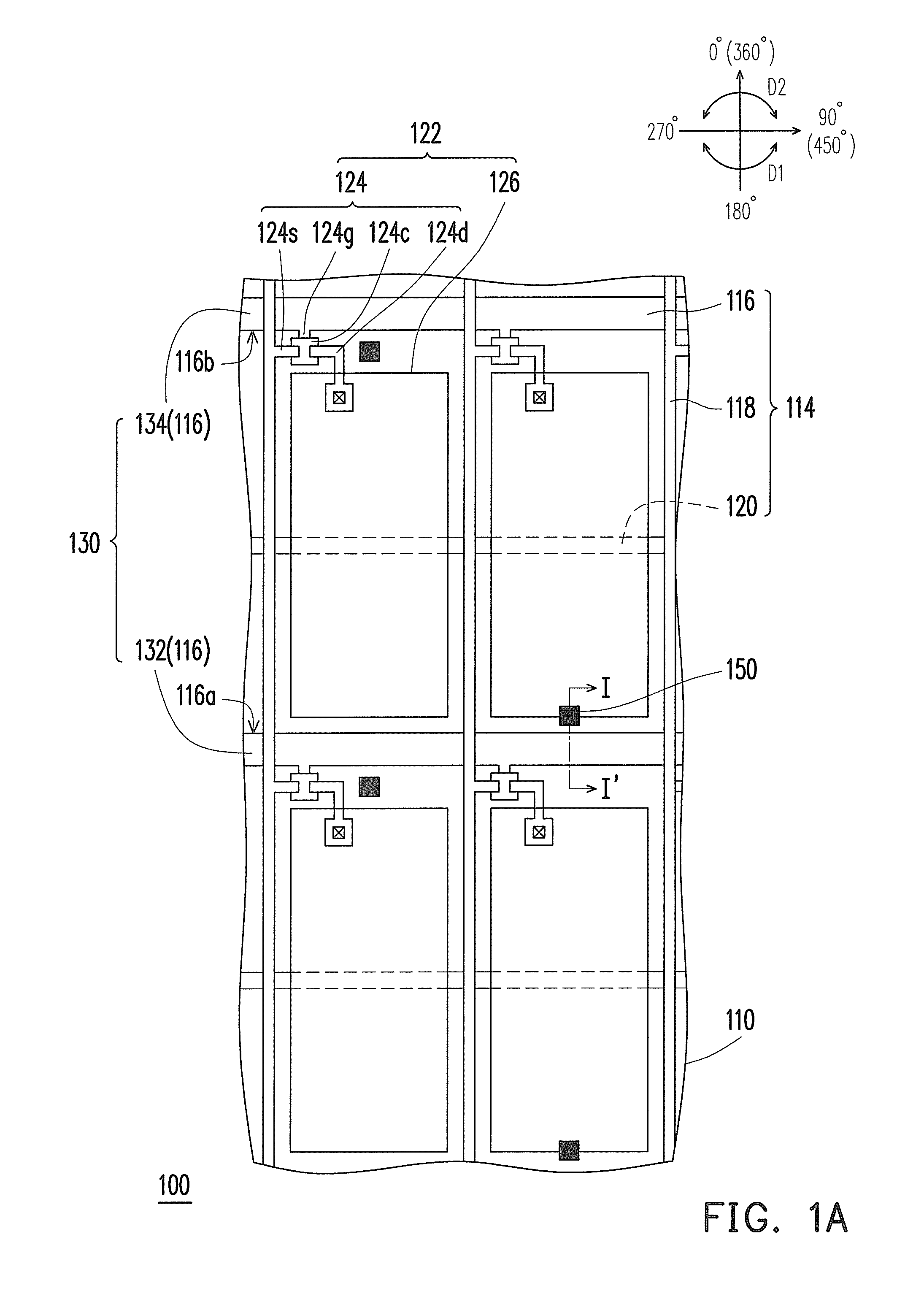
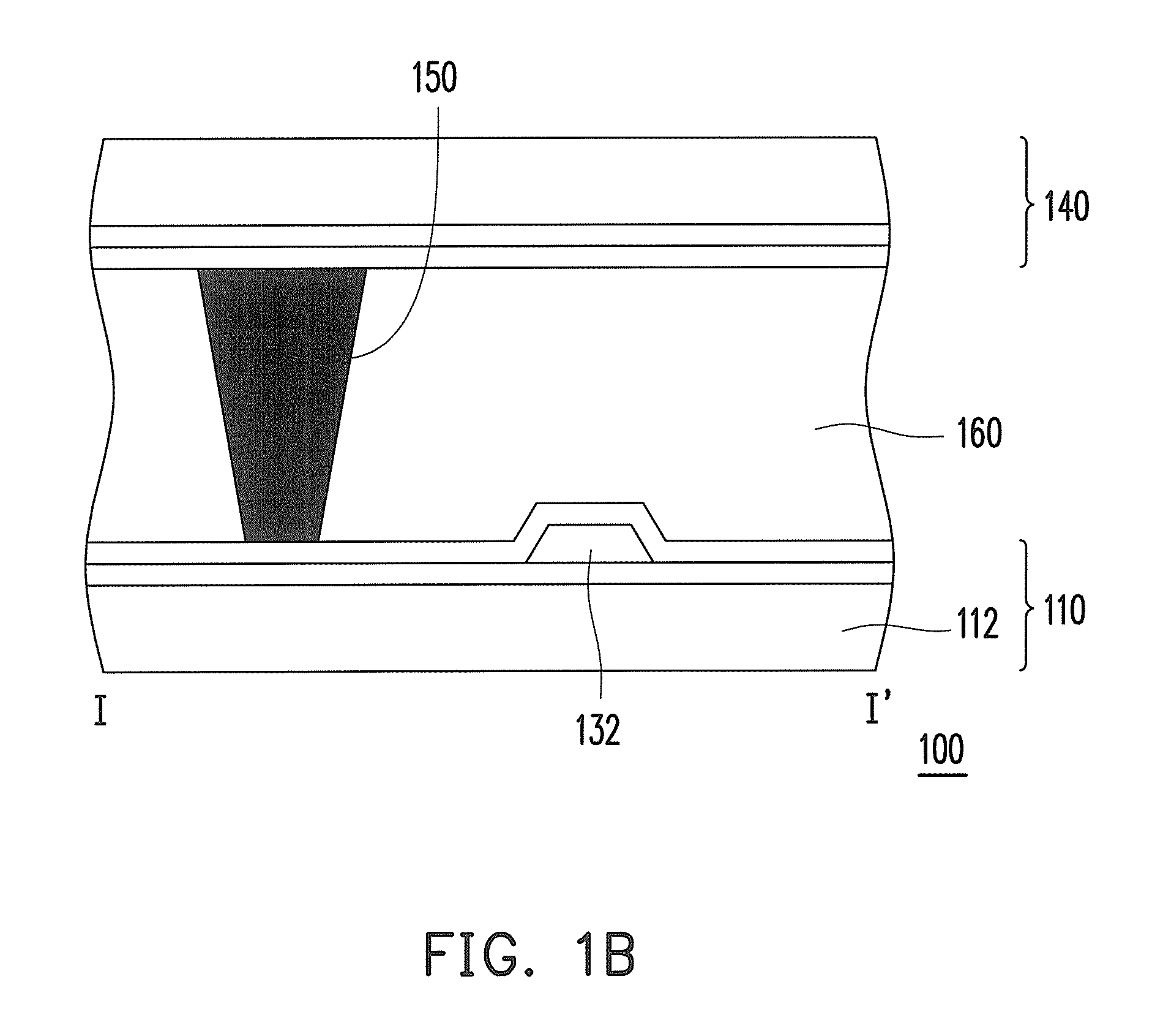
[0025]FIG. 1A is a schematic top view of a liquid crystal display (LCD) panel in accordance with an embodiment of the invention. FIG. 1B is a partial schematic cross-sectional view of FIG. 1A along a line I-I′. For clarity of illustration, an opposite substrate and a liquid crystal layer are not shown in FIG. 1A. Referring to FIGS. 1A and 1B, an LCD panel 100 according to the present embodiment includes an active device array substrate 110, an opposite substrate 140, a plurality of spacers 150, and a liquid crystal layer 160. The active device array substrate 110 includes a plurality of position limiting structures 130, in which each of the position limiting structures 130 includes a first position limiting pattern 132 and a second position limiting pattern 134. The opposite substrate 140 is disposed above the active device array substrate 110. The liquid crystal layer 160 is disposed between the active device array substrate 110 and the opposite substrate 140. The plurality of spac...


PUM

PropertyMeasurementUnit
displacementaaaaaaaaaa
conductiveaaaaaaaaaa
weightaaaaaaaaaa

Abstract

A liquid crystal display panel including an active device array substrate, an opposite substrate, a plurality of spacers and a liquid crystal layer is provided. The active device array substrate includes a plurality of position limiting structures, each including a first and a second position limiting pattern. The opposite substrate is disposed above the active device array substrate. The spacers are disposed on the opposite substrate, and the spacers are protruded towards the active device array substrate and extended adjacent to the first and second position limiting patterns. Displacement of each spacer is limited by the first or second position limiting pattern. The first position limiting patterns limit the displacement of a portion of the spacers along a first azimuth range, the second position limiting patterns limit the displacement of a portion of the spacers along a second azimuth range, and the first and second azimuth ranges are different.

Description

CROSS-REFERENCE TO RELATED APPLICATION[0001]This application claims the priority benefit of Taiwan application serial no. 99113291, filed on Apr. 27, 2010. The entirety of the above-mentioned patent application is hereby incorporated by reference herein and made a part of this specification.BACKGROUND OF THE INVENTION[0002]1. Field of the Invention[0003]The invention relates generally to a display panel, and more particularly to a liquid crystal display panel.[0004]2. Description of Related Art[0005]With advantages of high definition, small volume, light weight, low driving voltage, low power consumption, and an extensive range of applications, the liquid crystal display (LCD) has become the mainstream device among various display products. The conventional LCD panel is constituted by an active device array substrate, a color filter substrate, and a liquid crystal layer sandwiched therebetween. Moreover, photo spacers are disposed between the color filter substrate and the active de...

Claims


Application Information

Patent Timeline
Patent Type & Authority Patents(United States)
IPC IPC(8): G02F1/1339
CPCG02F1/13394
Inventor HUANG, WEI-KAIHSIEH, JEN-CHIEHTANG, LUNG-LING
Owner AU OPTRONICS CORP
Learn More