Method for simultaneously cutting a compound rod of semiconductor material into a multiplicity of wafers

a technology of compound rods and semiconductor materials, which is applied in the direction of manufacturing tools, chemistry apparatus and processes, transportation and packaging, etc., can solve the problems of insufficient use of inability to optimally use gang lengths of wire saws, and limited gang lengths. , to achieve the effect of improving the warp of the wafers

Active Publication Date: 2012-10-09
SILTRONIC AG
View PDF11 Cites 3 Cited by
  • Summary
  • Abstract
  • Description
  • Claims
  • Application Information

AI Technical Summary

Benefits of technology

[0013]An aspect of the present invention is to avoid such geometrical variations and, in particular, to improve the warp of the wafers fabricated from the compound rod.
[0023]Grinding the end surfaces so that the two end surfaces of the at least two workpieces, which adhesively bond together, are plane-parallel, allows the adhesive joint between the two rod pieces to be made as small as possible.
[0033]Assembling rod pieces to form a compound rod without using separating pieces, and subsequent sawing, results in an even higher economic viability compared with the prior art since the use of the wire saw is further improved.
[0034]On the other hand, the compound rod according to the invention behaves similarly as a single rod in the sawing process. The geometrical variations observed in the prior art can be avoided.
[0047]Essentially the workpieces are selected from a stock of workpieces, possibly of different lengths, so that the gang length of the wire saw is used optimally. Since no separating pieces are used, the adhesive joint between the assembled workpieces is minimal and the capacity of the wire saw is therefore utilized better, which further increases the productivity of the process compared with the prior art.

Problems solved by technology

This method has the crucial disadvantage that part of the gang length, which is limited by the dimensions of the wire saw, is used for cutting the “unused” dummy pieces.
Furthermore the provision, handling and adhesive bonding of dummy pieces is very elaborate and difficult to manage.
In the simultaneous cutting of a plurality of workpieces in a wire saw as described in U.S. Pat. No. 6,119,673, the gang length of the wire saw also cannot be used optimally since the workpieces to be cut have very different lengths owing to the way in which they are produced.
This problem arises in particular whenever the workpieces consist of monocrystalline semiconductor material, since the known crystal pulling processes only allow certain usable lengths of the crystals or, in order to monitor the crystal pulling processes—as already mentioned above—it is necessary to split the crystals and produce test samples at various positions of the crystal.
The disadvantages of the methods known from the prior art are found to be particularly significant for the bow and warp parameters as a measure of the deviation of the actual wafer shape from the desired ideal wafer shape (or “sori”).

Method used


Image

  • Method for simultaneously cutting a compound rod of semiconductor material into a multiplicity of wafers
  • Method for simultaneously cutting a compound rod of semiconductor material into a multiplicity of wafers
  • Method for simultaneously cutting a compound rod of semiconductor material into a multiplicity of wafers

Examples


Embodiment Construction

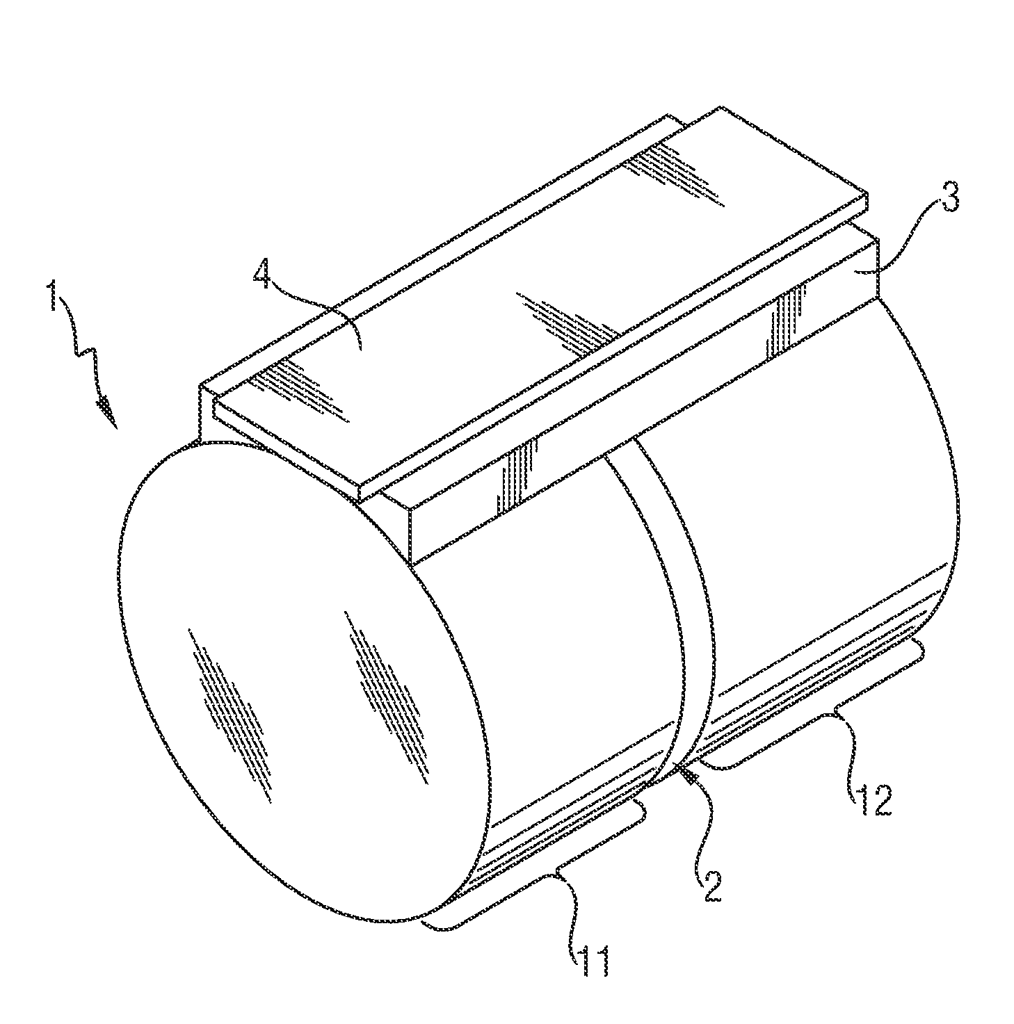
[0057]The workpieces 11 and 12 are assembled with a two-component adhesive to form a compound rod 1. The fabrication accuracy of the end surfaces, on which the two workpieces are adhesively bonded together, allows the adhesive joint 2 to be selected as small as possible. The workpieces 11 and 12 assembled to form a compound rod 1 are cemented onto a sawing strip 3. The compound rod 1 comprising the two workpieces 11 and 12 and with the sawing strip 3 is fixed on a mounting plate 4 and clamped in a wire saw.

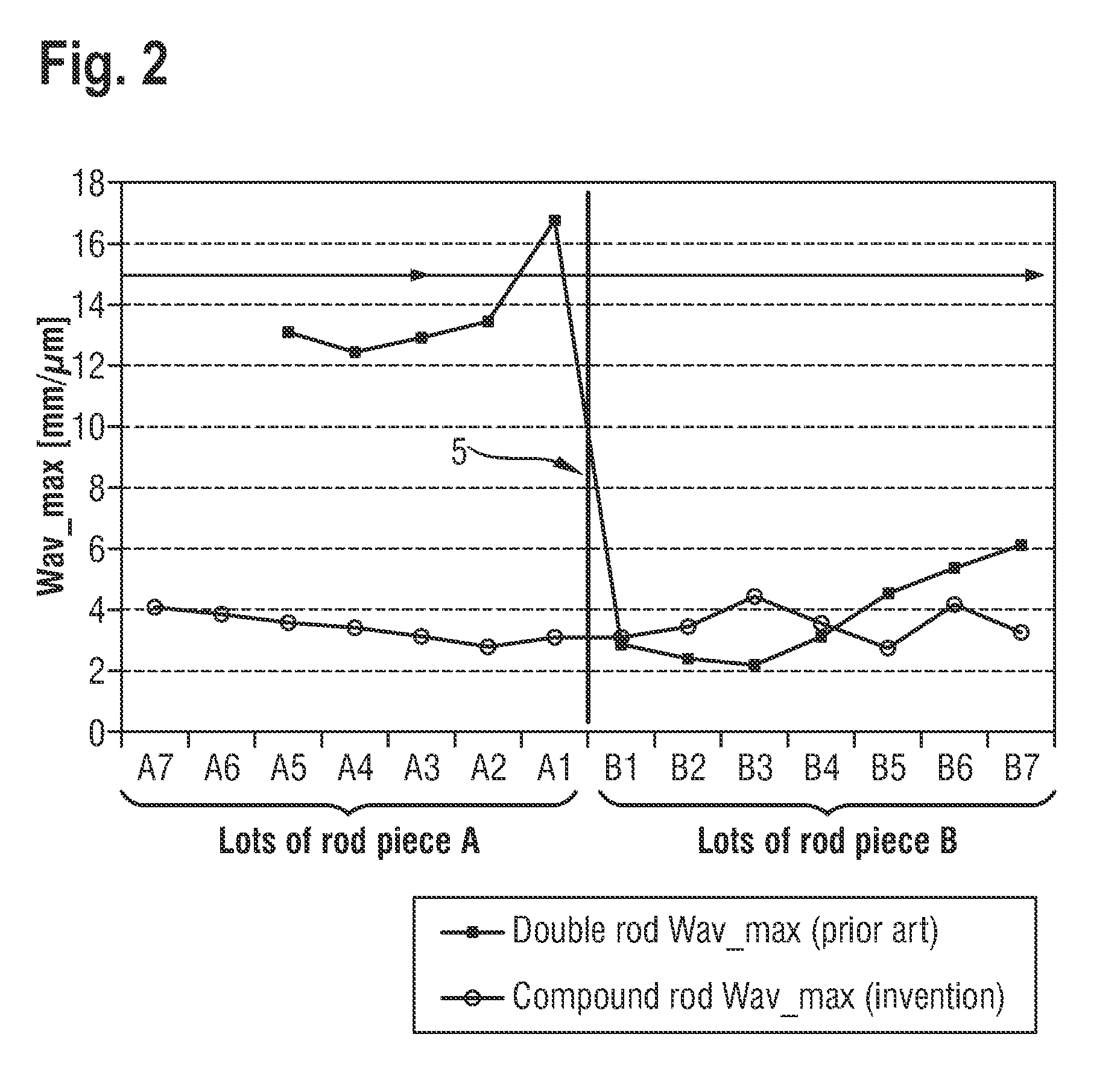
[0058]Table 1 shows various comparative values of geometrical parameters for assembled rod pieces according to the prior art (column 2) and for compound rods according to the invention (column 3).

[0059]Three values of three different quantile values are given for each parameter: thus, Wav_max 97.7%=6.29 μm / mm means that 97.7% of the wafers have a Wav_max of 56.29 μm / mm or less, etc.

[0060]A significant improvement over the prior art is found for virtually all studied parameters and...


PUM

PropertyMeasurementUnit
total lengthaaaaaaaaaa
lengthsaaaaaaaaaa
lengthsaaaaaaaaaa

Abstract

A method for simultaneously cutting a compound rod of semiconductor material into a multiplicity of wafers. The method includes selecting a first workpiece and a second workpiece, each having two end surfaces; grinding at least one of the two end surfaces of each workpiece so as to create a ground end surface on each workpiece; cementing the ground end surface of the first workpiece to the ground end surface of second workpiece using a fastener so as to produce a compound rod piece having a longitudinal axis, wherein the fastener is disposed between the workpieces so as create a distance between the workpieces; fixing the compound rod piece in a longitudinal direction on a mounting plate; clamping the mounting plate with the compound rod piece in a wire saw; and cutting the compound rod piece perpendicularly to the longitudinal axis using the wire saw.

Description

[0001]Priority is claimed to German Application No. DE 10 2008 051 673.2, filed on Oct. 15, 2008, the entire disclosure of which is incorporated by reference herein.[0002]The invention relates to a method for simultaneously cutting a compound rod of semiconductor material into a multiplicity of wafers.BACKGROUND[0003]Workpieces of semiconductor material are conventionally cut into wafers by means of a wire saw. Wire saws are used in the prior art to cut cylindrical mono- or polycrystalline workpieces of semiconductor material, for example silicon, simultaneously into a multiplicity of wafers in one working operation. The throughput of the wire saw is in this case of great importance for the economic viability of the method.[0004]Owing to the way in which they are produced, shorter and longer rod pieces are obtained in wafer production. It is also often necessary to cut rod portions from a single crystal, for example in order to examine the crystal properties. In order then to increa...

Claims


Application Information

Patent Timeline
Patent Type & Authority Patents(United States)
IPC IPC(8): B28D1/02B32B38/04
CPCB28D5/0082B28D5/045Y10T428/192Y10T156/1052Y10T83/0405H01L21/30
Inventor RIEGER, ALEXANDEROELKRUG, HANSSCHUSTER, JOSEF
Owner SILTRONIC AG
Why Eureka
Try Eureka