Method for separating support substrate from solid-phase bonded wafer and method for manufacturing semiconductor device

a technology of solid-phase bonding and support substrate, which is applied in the direction of transistors, electrical equipment, basic electric elements, etc., can solve the problems of increasing the cost of silicon wafer, increasing the cracking or the like of the wafer, and reducing the efficiency of silicon dust recycling, so as to achieve the effect of reducing the cost of wafer and separating the support substra

Active Publication Date: 2014-08-07
FUJI ELECTRIC CO LTD
View PDF71 Cites 3 Cited by
  • Summary
  • Abstract
  • Description
  • Claims
  • Application Information

AI Technical Summary

Benefits of technology

[0015]In the case where a Si wafer is inputted in a wafer process, it is said that the thickness of a wafer which can be processed without substantially causing any problem such as wafer cracking has a lower limit of wafer thickness at about 300 μm or more with a diameter of 6 inches or about 400 μm or more with a diameter of 8 inches. However, when a wafer thinner than the lower limit of the wafer thickness is inputted in a wafer process directly, the warp of the Si wafer increases. Accordingly, particularly at an exposure process, TTV (Total Thickness Variation) is too poor to obtain a good resolution. In addition, in high temperature processing such as impurity thermal diffusion, crystal defects easily occur due to deformation of the wafer. Moreover, even when a wafer whose wafer thickness is 300 μm with a diameter of 6 inches or a wafer thickness of 400 μm with a diameter of 8 inches satisfying the lower limit of the aforementioned range is ground, for example, to be further thinned to a finished wafer thickness of 100 μm, two thirds or three fourths of the original wafer thickness has to be removed by the grinding. In other words, when a wafer having a finished thickness or a wafer having a thickness close to the finished thickness is used from an initial stage of a wafer process, it is obvious that saving the material and simplifying the grinding step can be achieved and the cost can be also reduced. Also in the case of the reinforcing rib system wafer, the center portion of the back surface of the wafer excluding the outer circumferential portion is hollowed out. Accordingly, the ratio of the part removed by grinding is not much different from the aforementioned case.SUMMARY OF THE INVENTION
[0016]The invention has been accomplished in consideration of the aforementioned points. The invention provides a method for separating a support substrate from a solid-phase bonded wafer and a method for manufacturing a semiconductor device, capable of using a Si wafer without substantial wafer cracking from an initial stage of a wafer process, capable of separating a support substrate from the Si wafer easily, and capable of reducing the wafer cost.
[0019]According to the invention, it is possible to provide a method for separating a support substrate from a solid-phase bonded wafer and a method for manufacturing a semiconductor device, capable of using a Si wafer without substantial wafer cracking from an initial stage of a wafer process, capable of separating a support substrate from the Si wafer easily, and capable of reducing the wafer cost.

Problems solved by technology

In fact, however, wafer cracking or the like increases easily due to stress caused by heat when a thin wafer is inputted in the initial stage of the process.
Therefore, the silicon dust cannot be recycled.
According to the temporary pasting system for pasting a support substrate to the back surface of a wafer with an adhesive agent, high temperature processing cannot be performed after the adhesion.
However, this technique is originally not based on the assumption that the support substrate will be separated again.
Therefore, there is a problem in the fact that a method for easily separating the support substrate from the solid-phase bonded Si wafer has not been put into practice yet.
According to the stealth dicing technique, however, such chipping is hardly observed either in the back side or in the front side.

Method used


Image

  • Method for separating support substrate from solid-phase bonded wafer and method for manufacturing semiconductor device
  • Method for separating support substrate from solid-phase bonded wafer and method for manufacturing semiconductor device
  • Method for separating support substrate from solid-phase bonded wafer and method for manufacturing semiconductor device

Examples


example 1

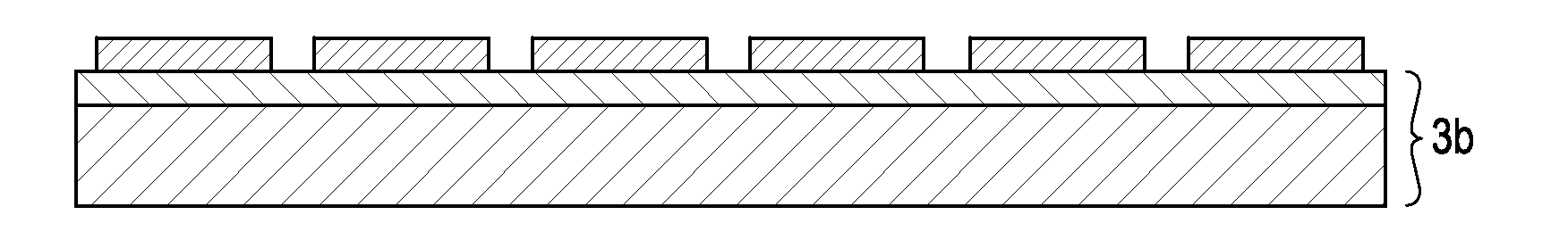
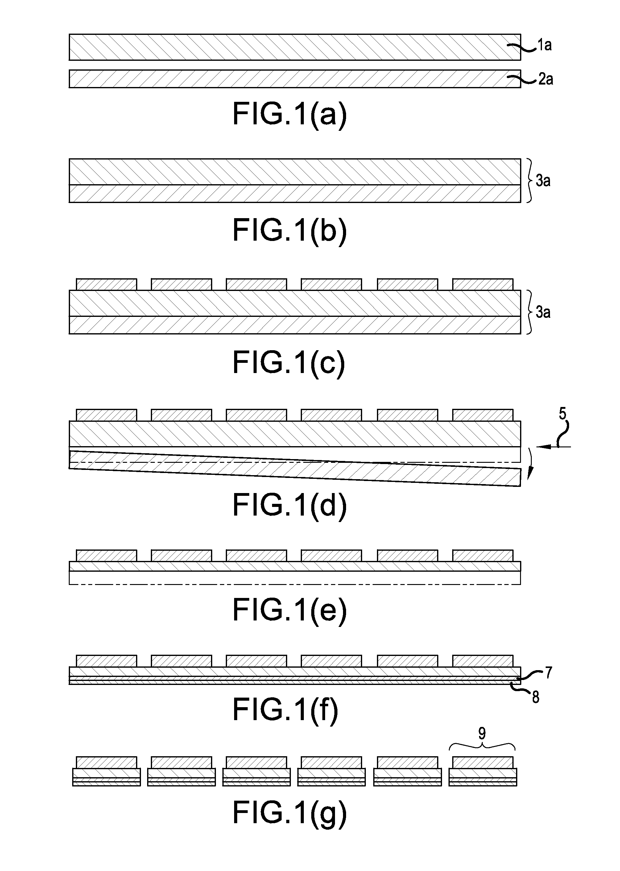
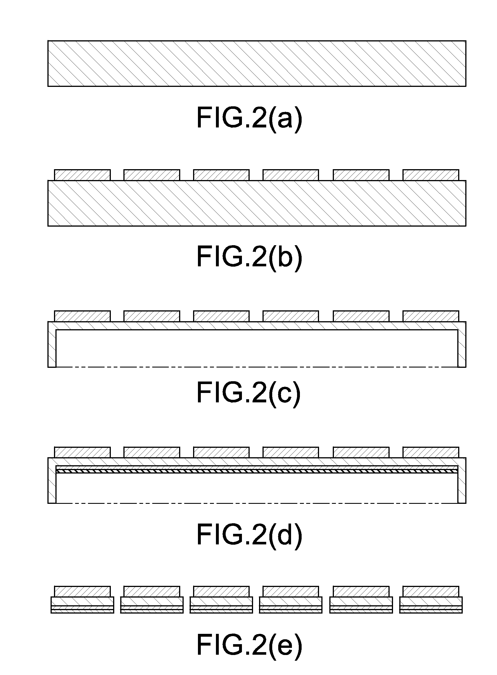
[0057 of the method for manufacturing a semiconductor device using the method for separating a support substrate from a solid-phase bonded wafer according to the invention will be described in detail with reference FIG. 1. FIG. 1 includes sectional views, all of which show wafers. CZ-p type Si support wafer 2a having a diameter of 8 inches and a thickness of 300 μm is prepared as a support substrate for FZ-n type Si wafer 1a having the same diameter and a thickness less than 400 μm (FIG. 1(a)). Here, Si wafer 1b with a thickness of 100 μm and support wafer 2b with a thickness of 700 μm may be prepared alternatively, as shown in FIG. 4(a). In FIG. 4, Si solid-phase bonded wafer 3b is used. In Si solid-phase bonded wafer 3b, Si wafer 1b having a thickness of 100 μm substantially corresponding to the thickness of a finished wafer and support wafer 2b having a thickness of 700 μm are bonded to each other by solid-phase bonding. Accordingly, the method in FIG. 4 is the same as the method...


PUM


Abstract

A method is disclosed for separating a support substrate from a solid-phase bonded wafer which includes a Si wafer and support substrate solid-phase bonded to back surface of the Si wafer. The method includes a step of irradiating the Si wafer with laser light with a wavelength which passes through the Si wafer and is focused on a solid-phase bonding interface between the Si wafer and support substrate to form a breaking layer in at least part of an outer circumferential portion of the solid-phase bonding interface, a step of separating the breaking layer; and a step of separating the solid-phase bonding interface. The method is capable of using a Si thin wafer without substantial wafer cracking at an initial stage where the wafer is inputted to a wafer process, capable of separating a support substrate from the Si thin wafer easily, and capable of reducing the wafer cost.

Description

BACKGROUND OF THE INVENTION[0001]A. Field of the Invention[0002]The present invention relates to a WSS (Wafer Support System) wafer (solid-phase bonded wafer), and particularly relates to a method for separating a support substrate from the WSS wafer and a method for manufacturing a semiconductor device using this method.[0003]B. Description of the Related Art[0004]As to a power device such as an IGBT (Insulated Gate Bipolar Transistor), it has been recognized that reduction in the thickness of a semiconductor substrate has a great advantage in view of characteristics such as reduction in energy loss, heat dissipation, etc. As for the reduction in the thickness of a semiconductor substrate, highest manufacturing efficiency can be obtained if a semiconductor device can be manufactured using a wafer (thin wafer) which is already thin in an initial stage where the wafer is inputted to a process. To this end, there is a strong need to establish a wafer process in which a thin wafer can ...

Claims


Application Information

Patent Timeline
Patent Type & Authority Applications(United States)
IPC IPC(8): H01L21/762
CPCH01L21/76254H01L21/187H01L29/66333H01L21/84H01L21/6836H01L21/7806H01L21/78
Inventor NAKAJIMA, TSUNEHIRO
Owner FUJI ELECTRIC CO LTD
Why Eureka
Try Eureka