Method for making an electric interconnection between two conducting layers

a technology of conducting layer and electric interconnection, which is applied in the direction of printed circuit aspects, electrical apparatus, coatings, etc., can solve the problems of difficult to formulate ink appropriate for printing techniques, danger of affecting the electrical performance of transistors, and use of dielectric or semi-conducting materials

Active Publication Date: 2012-10-16
COMMISSARIAT A LENERGIE ATOMIQUE ET AUX ENERGIES ALTERNATIVES
View PDF5 Cites 2 Cited by
  • Summary
  • Abstract
  • Description
  • Claims
  • Application Information

AI Technical Summary

Benefits of technology

[0033]Moreover, the directional pitch of the sides of the stud has an effect on the non-wettability of the insulation or semi-conducting layer at this level. Typically, the pitch of the sides and in particular the value of the angle α between the horizontal and the sides is advantageously between 45 and 135°.

Problems solved by technology

Such pollutions prove in fact to be particularly critical when they affect the semi-conductor / insulator interface, and may be severely detrimental to the electrical performance of the transistors.
Moreover, the accumulation of steps at the end of the process increases the danger of causing impairment to the layers already deposited, such impairment translating in particular into the disbonding of the layers after laser firing, or even the unintentional dissolution of part of the layers when the vias are made by jets of solvent, etc.
However, experience shows that the use of some dielectric or semi-conducting materials is difficult to formulate in an ink appropriate for printing techniques.
Moreover, these deposition methods do not provide sufficient spatial resolution in a large number of applications.

Method used


Image

  • Method for making an electric interconnection between two conducting layers
  • Method for making an electric interconnection between two conducting layers
  • Method for making an electric interconnection between two conducting layers

Examples


Embodiment Construction

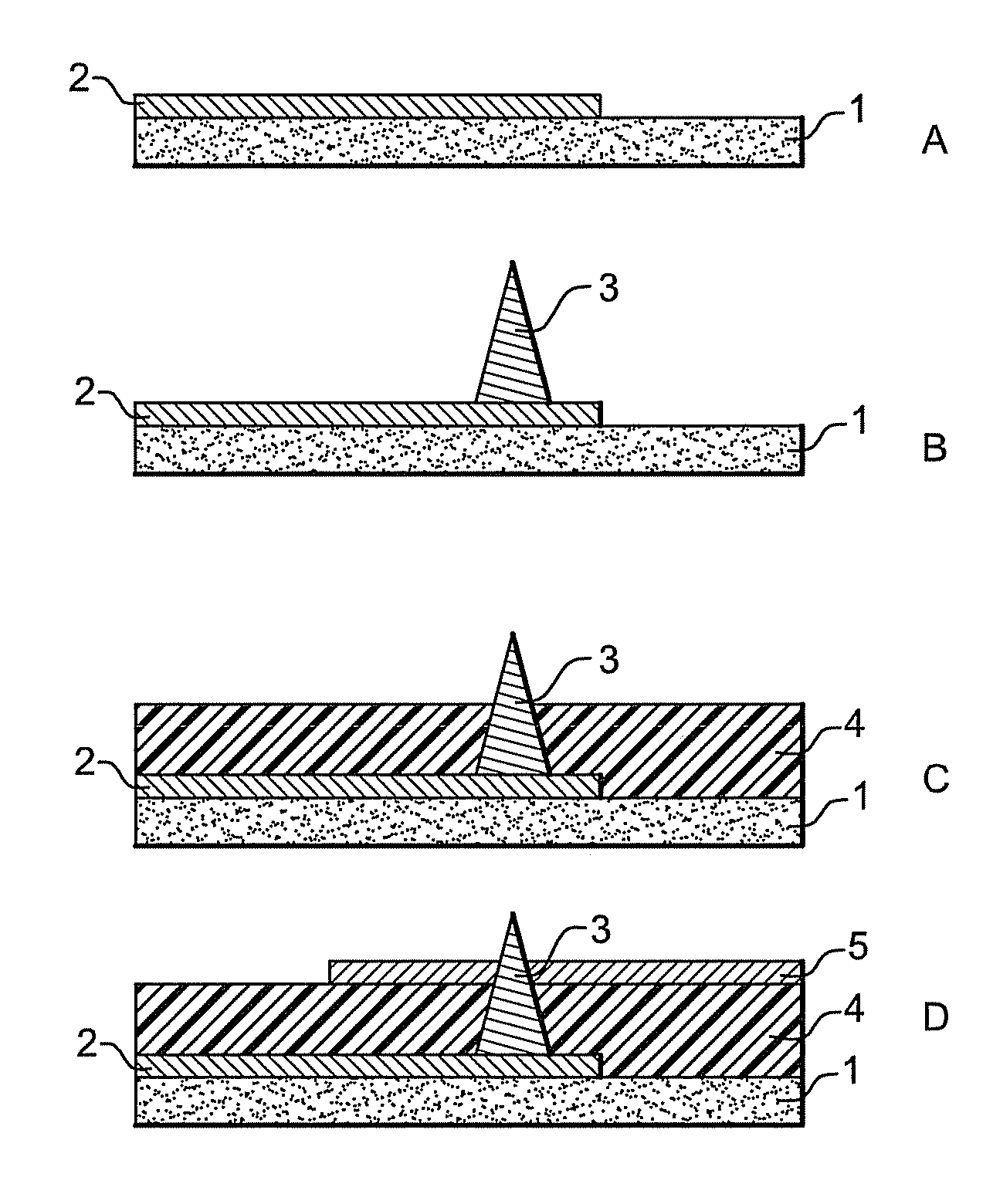
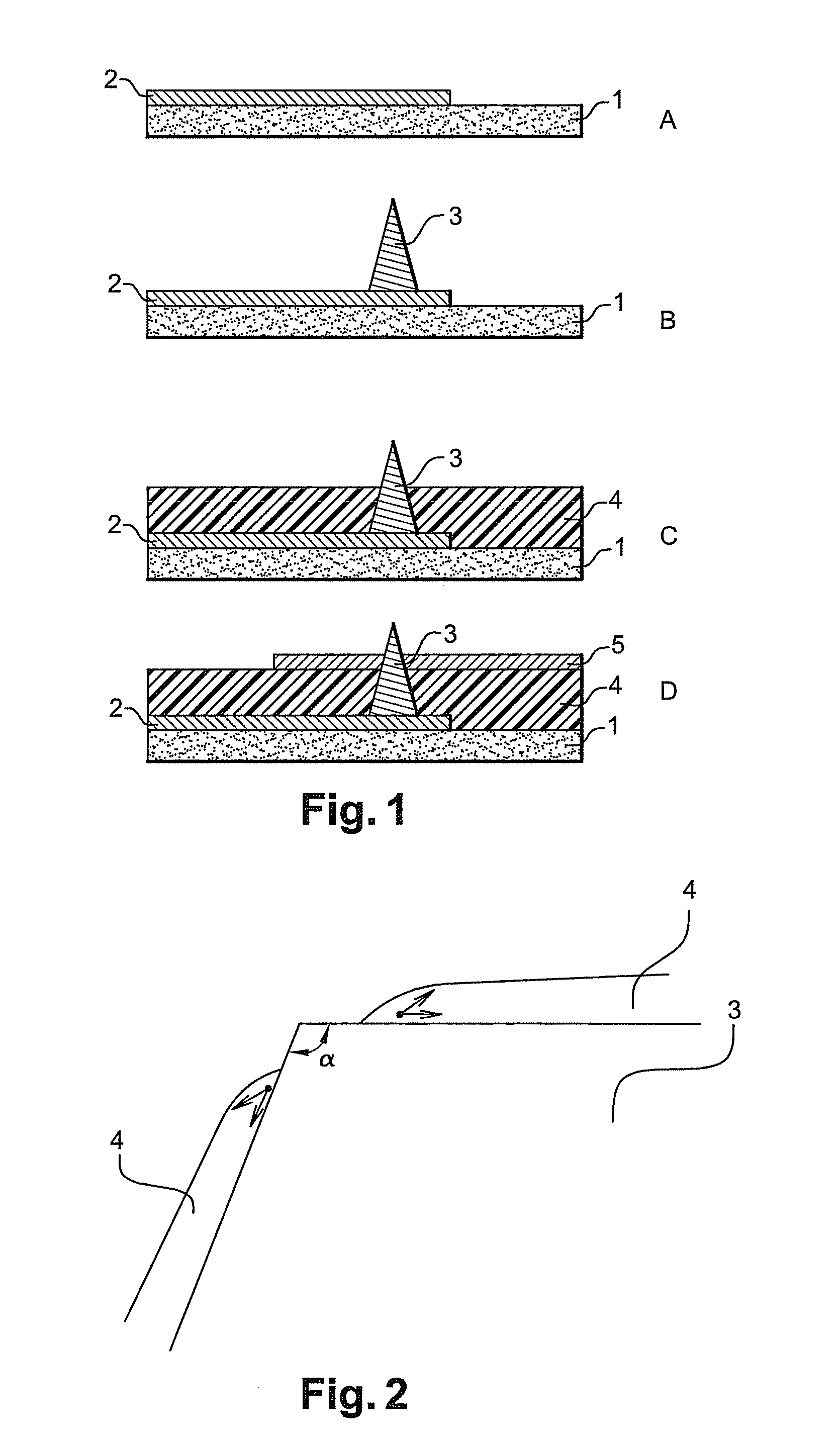
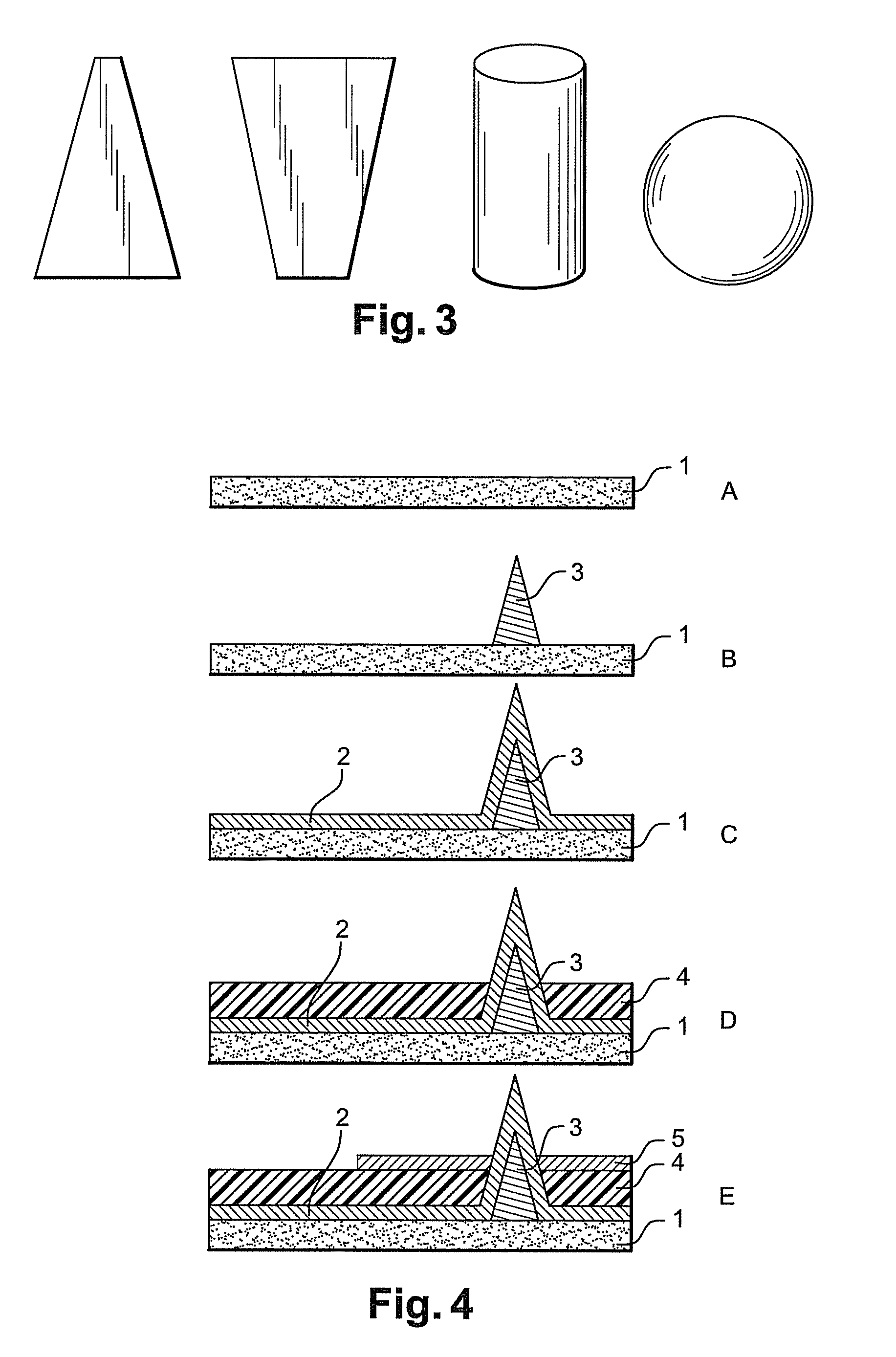
[0046]As will have been understood, the present invention proposes two possible methods for making a via to interconnect two conducting layers 2, 5, separated by an insulation or semi-conducting layer 4.

[0047]According to the invention, this via is implemented by forming a stud 3, added on to the lower conducting layer 2 or directly onto the substrate 1, on which the lower conducting layer is deposited, or emanating from this lower conducting layer.

[0048]Depending on the conducting or non-conducting nature of the initial stud 3, different methods are conceivable.

[0049]According to a first method intended to form a stud that is directly conducting, in other words wherein the nature of its constituent material is conducting, and made for example out of Au, Cu, Ag or conducting polymers such as PDOT-PSS (poly(3,4-ethylenedioxythiphene) polystyrenesulphonate), the geometry of the first lower conducting layer 2 is modified.

[0050]This layer 2 is conventionally deposited onto a substrate 1...


PUM


Abstract

A method for making an electric interconnection between two conducting layers, separated by at least one insulation or semi-conducting layer, which includes forming a stud extending between at least the lower conducting layer and the upper conducting layer, where the nature and / or the shape of the stud impart non-wettability properties relative to the material used for the separating layer.

Description

FIELD OF THE INVENTION[0001]The present invention relates to the making of an electric interconnection between two conducting layers separated by at least one insulation or semi-conducting layer, as implemented most specifically in the manufacture of electronic circuits.[0002]It can be used in particular when the separating layer of insulation or semi-conducting material is deposited by a wet process.[0003]The conventional term is a via which, in a known way, constitutes a conducting path through an insulation layer.[0004]The present invention applies most specifically to the making of transistors, for which the via in question constitutes the conducting path through the gate insulator and the semi-conductor.[0005]It can also be used in a general way to make vias in the context of electronics that use organic and inorganic materials and / or hybrid organic-inorganic materials, in particular deposited by a wet process.BACKGROUND OF THE INVENTION[0006]Two methods may conventionally be d...

Claims


Application Information

Patent Timeline
Patent Type & Authority Patents(United States)
IPC IPC(8): H01L21/44
CPCH05K3/0017H05K3/4084H05K3/4647H05K3/4664H01L21/76885H05K2203/128H05K2201/091H05K2201/09909H05K2203/107H05K2203/1173
Inventor VERILHAC, JEAN-MARIEBABLET, JACQUELINEBORY, CECILE
Owner COMMISSARIAT A LENERGIE ATOMIQUE ET AUX ENERGIES ALTERNATIVES
Why Eureka
Try Eureka