Supercharge Your Innovation With Domain-Expert AI Agents!

Semiconductor device including over voltage protection circuit having gate discharge circuit operated based on temperature and voltage as to output transistor

a technology of over voltage protection circuit and output transistor, which is applied in the direction of emergency protective arrangements for limiting excess voltage/current, electronic switching, pulse technique, etc., can solve the problems of short circuit, short circuit, and short circuit of gate discharge circuit to turn off the first transistor tb>1/b>

Active Publication Date: 2012-10-16
RENESAS ELECTRONICS CORP
View PDF6 Cites 4 Cited by
  • Summary
  • Abstract
  • Description
  • Claims
  • Application Information

AI Technical Summary

Benefits of technology

[0023]With the above-described circuit configuration, it is possible to control a variation in potential difference of an output transistor caused by a load inductance component or the like.
[0024]According to the exemplary aspect of the present invention, it is possible to provide a semiconductor device capable of controlling a variation in potential difference of an output transistor caused by a load inductance component or the like.

Problems solved by technology

The breakdown current degrades the output transistor, which is problematic.
Note that, as will be described below, a problem may occur if the first transistor T1 is turned off (the first transistor T1 is controlled to switch from an on state to an off state) at high speed during a process in which the operation shown in FIG. 7 shifts from [f] to [g].
This may break down the first transistor T1, which is problematic.
That is, it takes long time to turn off the first transistor T1.

Method used


Image

  • Semiconductor device including over voltage protection circuit having gate discharge circuit operated based on temperature and voltage as to output transistor
  • Semiconductor device including over voltage protection circuit having gate discharge circuit operated based on temperature and voltage as to output transistor
  • Semiconductor device including over voltage protection circuit having gate discharge circuit operated based on temperature and voltage as to output transistor

Examples


first exemplary embodiment

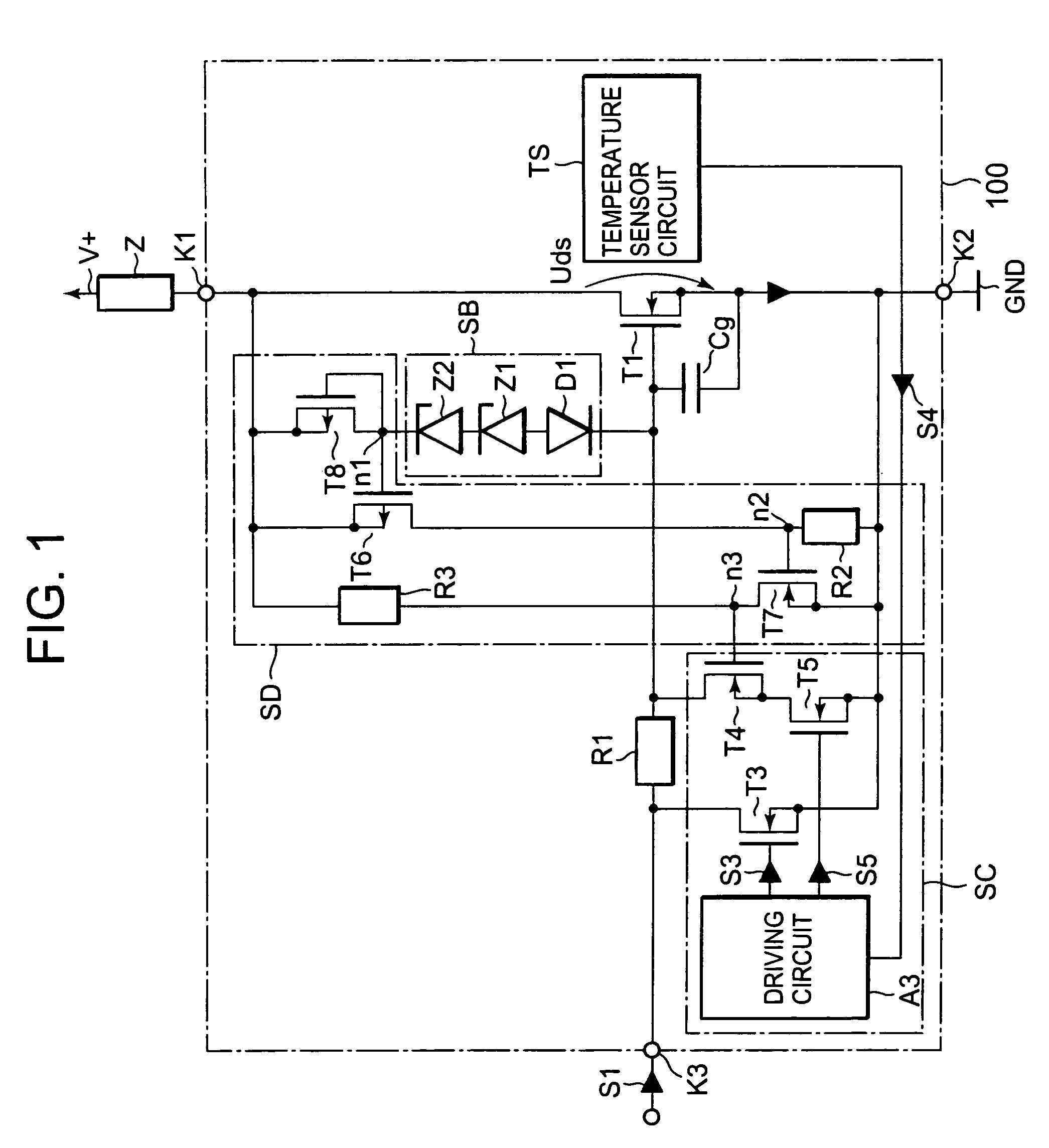
[0035]FIG. 1 shows a circuit diagram of a semiconductor device according to a first exemplary embodiment. As shown in FIG. 1, a semiconductor device 100 includes a first terminal K1, a second terminal K2, a load Z, a first transistor (an output transistor in Claims for the patent) T1, a control input terminal K3, a voltage control circuit SB, a gate discharge circuit SC, a temperature sensor circuit TS, and a voltage control detection circuit SD.

[0036]The first terminal K1 is connected to one terminal of the load Z. The other terminal of the load Z is connected to a first power supply (high-side power supply) V+. The second terminal K2 is connected to a second power supply (low-side power supply) GND. A driving signal S1 is supplied to the semiconductor device 100 through the control input terminal K3. The first transistor T1 is, e.g., an n channel type power MOSFET. A drain of the first transistor T1 is connected to the first terminal K1. A source of the first transistor T1 is conn...

second exemplary embodiment

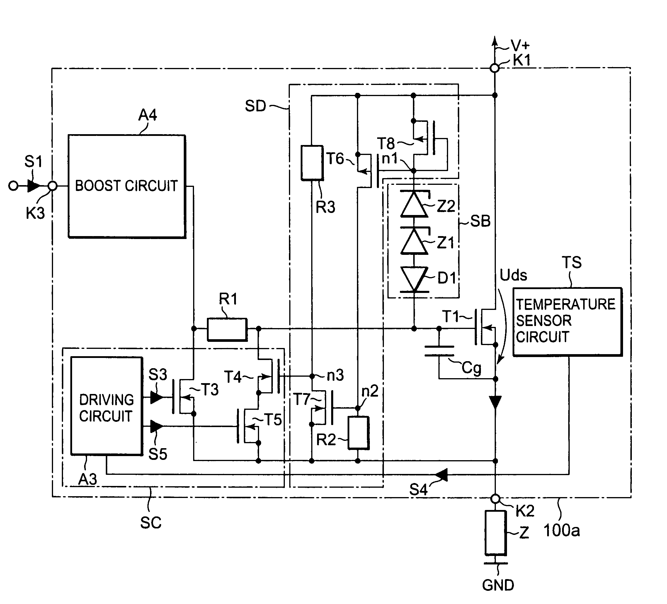
[0063]A second exemplary embodiment of the present invention will be described in detail with reference to the drawings. A semiconductor device 100a shown in FIG. 3 is different from the semiconductor device 100 in FIG. 1 described in the first exemplary embodiment of the present invention in a position where a load Z is connected. A first power supply V+ is connected to a first terminal K1 while a second power supply GND is connected to a second terminal K2 through the load Z. That is, the semiconductor device 100a adopts a high-side switch configuration (hereinafter referred to as a “high-side configuration”). The semiconductor device 100a further includes a boost circuit A4, and the on-off state of a first transistor T1 is controlled by a voltage boosted by the boost circuit A4. The other part of the circuit configuration is the same as the first exemplary embodiment, and a description thereof will be omitted.

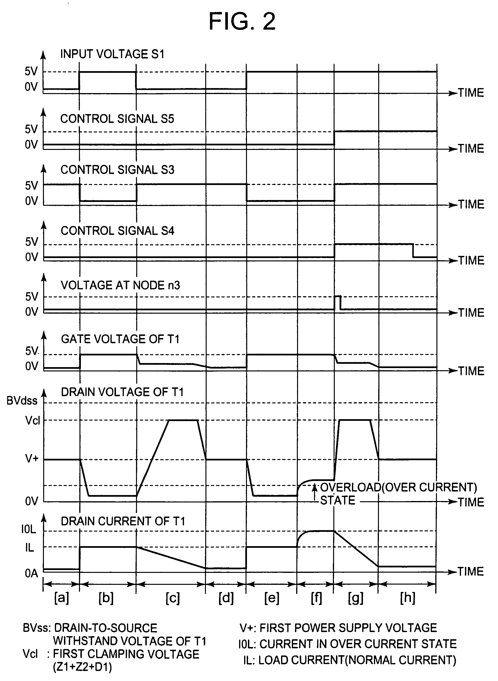
[0064]FIG. 4 illustrates timing charts showing the operation of the sem...


PUM


Abstract

A semiconductor device includes an output transistor which controls a power supply to a load according to a control voltage applied to a gate thereof, a voltage control circuit coupled between the gate and a drain of the output transistor, the voltage control circuit having a conduction state controlled according to a potential difference between a source and the drain of the output transistor, and a voltage control detection circuit which outputs a voltage control detection signal on a basis of the conduction state of the voltage control circuit. A first discharge switch is connected between the gate and the source of the output transistor, an on-off state of the first discharge switch being controlled according to the voltage control detection signal, a second discharge switch is series-connected to the first discharge switch between the gate and the source of the output transistor, an on-off state of the second discharge switch being controlled according to a temperature condition of the output transistor, and a third discharge switch is connected in parallel with the first and second discharge switches.

Description

[0001]This application is based upon and claims the benefit of priority from Japanese Patent Application No. 2008-304161 which was filed on Nov. 28, 2008, the disclosure of which is incorporated herein in its entirety by reference.BACKGROUND OF THE INVENTION[0002]1. Field of the Invention[0003]The present invention relates to a semiconductor device and, more particularly, to an overvoltage protection circuit.[0004]2. Description of Related Art[0005]Demand for an increase in surge breakdown voltage in a power switch for automotive electrical equipment has been growing in recent years. For example, an inductance load such as a solenoid or an inductance component of a wire harness is connected to an output stage of a power switch for automotive electrical equipment. If an inductance load is connected to an output stage of a power switch, as described above, a back electromotive force is generated when the power switch is turned off. The voltage of a voltage surge corresponding to the b...

Claims


Application Information

Patent Timeline
Patent Type & Authority Patents(United States)
IPC IPC(8): H02H9/04
CPCH03K17/0822H03K17/166H03K2017/0806
Inventor NAKAHARA, AKIHIRO
Owner RENESAS ELECTRONICS CORP
Features
  • R&D
  • Intellectual Property
  • Life Sciences
  • Materials
  • Tech Scout
  • Unparalleled Data Quality
  • Higher Quality Content
  • 60% Fewer Hallucinations
Learn More