Plasma processing apparatus

a processing apparatus and plasma technology, applied in the direction of chemical vapor deposition coating, electric discharge tubes, coatings, etc., can solve the problems reducing the energy of ions bombarding the focus ring, and relative difficulty in passing through the propagation path, so as to improve the plasma density distribution of the semiconductor wafer w, the effect of suppressing the consumption of the focus ring

Active Publication Date: 2012-10-30
TOKYO ELECTRON LTD
View PDF10 Cites 17 Cited by
  • Summary
  • Abstract
  • Description
  • Claims
  • Application Information

AI Technical Summary

Benefits of technology

[0006]In view of the above, the present invention provides a plasma processing apparatus capable of effectively suppressing a consumption of a focus ring without substantially affecting processes.
[0008]With such configuration, the peripheral dielectric member has a smaller electrostatic capacitance per unit area and a higher impedance than those of the main dielectric member. Therefore, in the case of a second high frequency, it is relatively difficult to pass through a propagation path of the peripheral dielectric member and the focus ring, and is relatively easy to pass through a propagation path of the main dielectric member and the substrate. As a consequence, the electric field in the ion sheath formed on the focus ring becomes relatively weak, thus decreasing the energy of ions bombarding the focus ring and suppressing the consumption of the focus ring.
[0013]A second high frequency power supply unit may apply to the first electrode a second high frequency power having a second frequency lower than the first frequency. In that case, as for the frequency (first frequency) of the first high frequency power, a frequency suitable for plasma generation is selected. Also, as for the frequency (second frequency) of the second high frequency power, a frequency suitable for ion attraction is selected. The effects of the embodiment of present invention are more apparent in the second high frequency than in the first high frequency. Namely, it is difficult for the relatively low second frequency to pass through the propagation path of the peripheral dielectric member and the focus ring due to the high impedance thereof. Hence, the ion bombardment on the focus ring can be suppressed and, further, the consumption of the focus ring can be effectively suppressed.
[0017]With such configuration, the second high frequency power having a relatively low frequency is applied to the main lower electrode without being applied to the peripheral lower electrode. Therefore, the ions are attracted from the plasma to the substrate on the main lower electrode and, also, the focus ring on the peripheral lower electrode can be prevented from the ion bombardment. Meanwhile, the first high frequency power having a relatively high frequency is divided and transmitted toward the processing space via the propagation path of the main lower electrode and that of the peripheral lower electrode and, then, the processing gas is plasma-excited above the focus ring as well as above the substrate. Since the plasma is generated above the focus ring as well as above the substrate, the characteristics of the plasma density distribution on the semiconductor wafer W are improved.
[0018]In accordance with the above-described configuration and operation of the plasma processing apparatus of the present invention, the consumption of the focus ring can be suppressed without substantially affecting the processes.

Problems solved by technology

Therefore, in the case of a second high frequency, it is relatively difficult to pass through a propagation path of the peripheral dielectric member and the focus ring, and is relatively easy to pass through a propagation path of the main dielectric member and the substrate.
As a consequence, the electric field in the ion sheath formed on the focus ring becomes relatively weak, thus decreasing the energy of ions bombarding the focus ring and suppressing the consumption of the focus ring.

Method used


Image

  • Plasma processing apparatus
  • Plasma processing apparatus
  • Plasma processing apparatus

Examples


Embodiment Construction

[0036]Hereinafter, embodiments of the present invention will be described with reference to FIGS. 1 to 15 which form a part hereof.

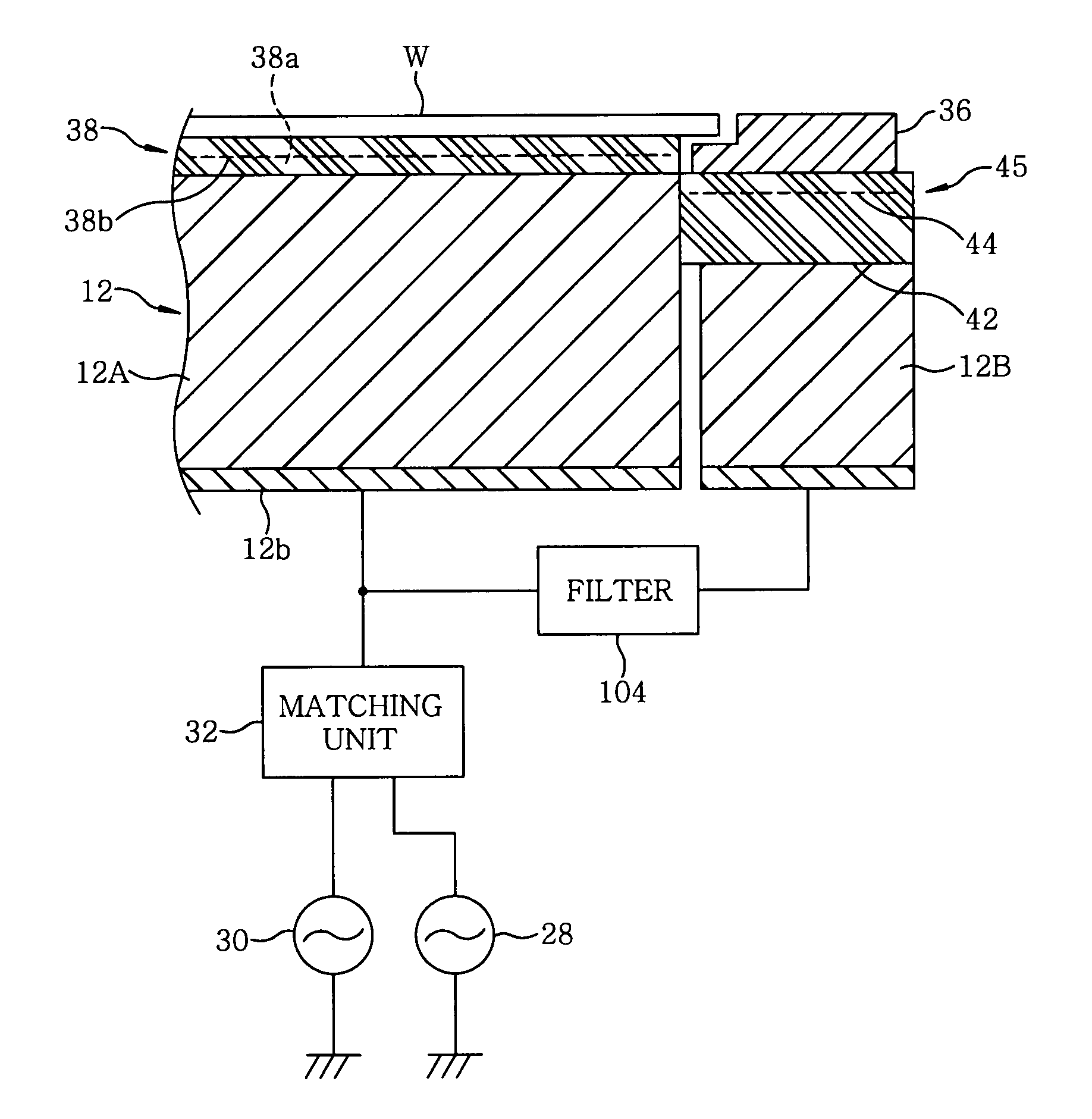
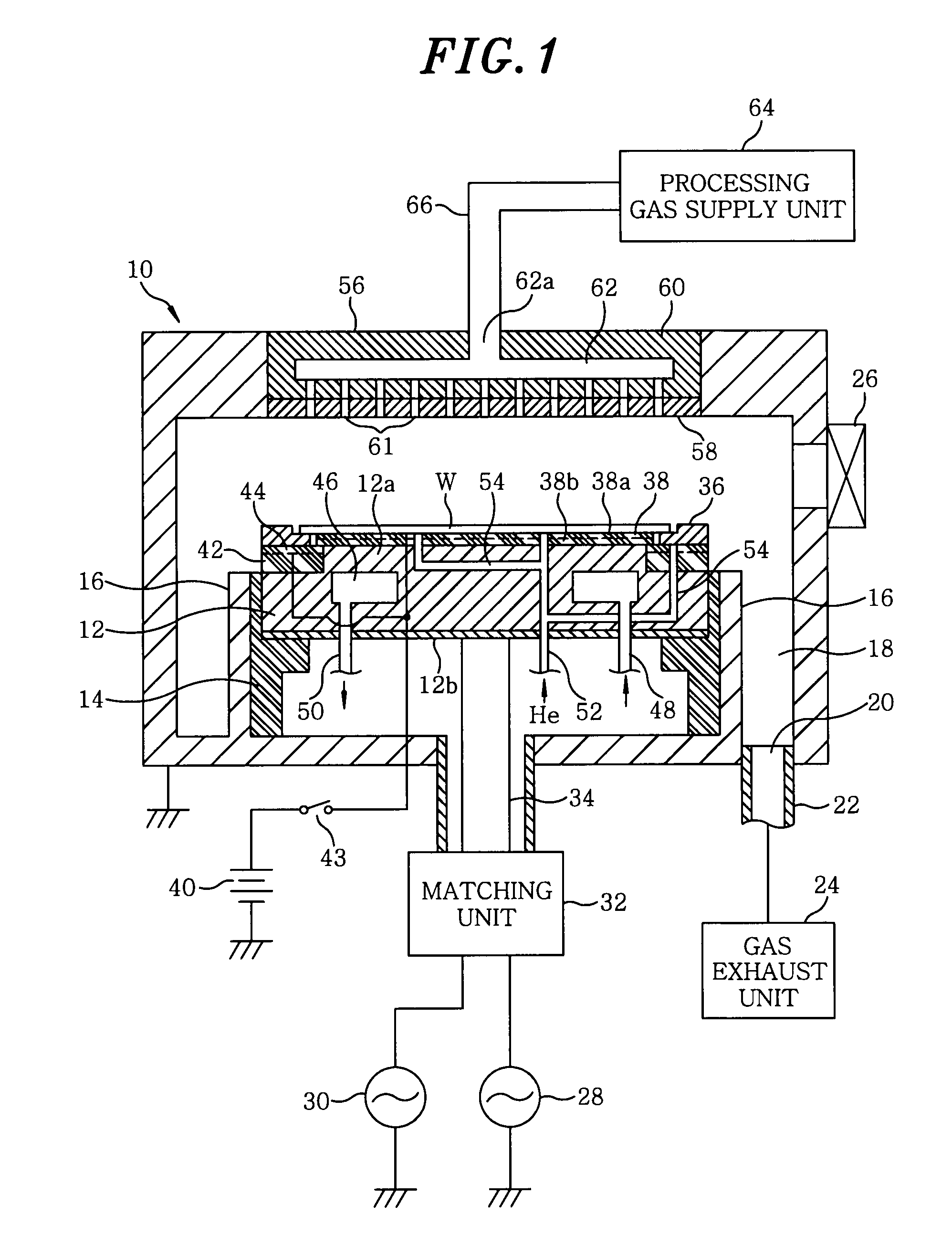
[0037]FIG. 1 is a vertical cross sectional view showing a configuration of a plasma etching apparatus in accordance with an embodiment of the present invention. This plasma etching apparatus is constructed as a capacitively coupled cathode couple plasma etching apparatus, and includes a cylindrical chamber (processing chamber) 10 made of a metal such as aluminum, stainless steel or the like. The chamber 10 is frame grounded.

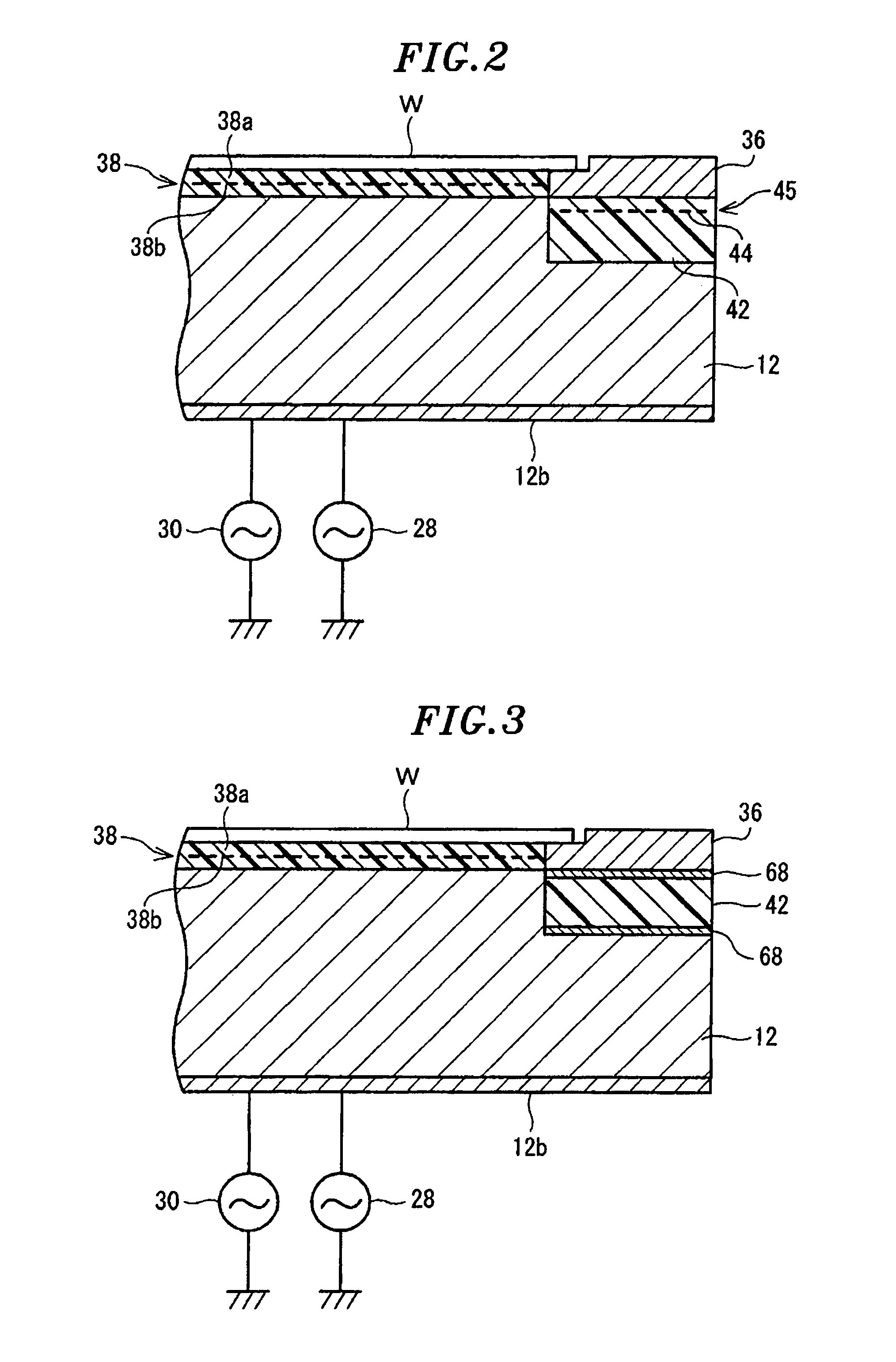
[0038]A circular plate-shaped susceptor 12 serving as a lower electrode for mounting thereon a target substrate, e.g., a semiconductor wafer W, is horizontally arranged in the chamber 10. The susceptor 12 has a main body or a base 12a made of, e.g., aluminum, and a conductive RF plate 12b fixed to a bottom surface of the base 12a. Further, the susceptor 12 is supported by a cylindrical insulating supporting portion 14 extending vertic...


PUM

PropertyMeasurementUnit
frequencyaaaaaaaaaa
frequencyaaaaaaaaaa
frequenciesaaaaaaaaaa

Abstract

A plasma processing apparatus includes a processing chamber, a first electrode and a second electrode disposed to face each other, a high frequency power supply unit for applying a high frequency power to either the first electrode or the second electrode, a processing gas supply unit for supplying a processing gas to a processing space, and a main dielectric member provided at a substrate mounting portion on a main surface of the first electrode. A focus ring is attached to the first electrode to cover a peripheral portion of the main surface of the first electrode and a peripheral dielectric member is provided in a peripheral portion on the main surface of the first electrode so that an electrostatic capacitance per unit area applied between the first electrode and the focus ring is smaller than that applied between the first electrode and the substrate by the main dielectric member.

Description

FIELD OF THE INVENTION[0001]The present invention relates to a technique for performing a plasma processing on a target substrate; and, more particularly, to a capacitively coupled plasma processing apparatus in which a focus ring is attached to an electrode for supporting a substrate.BACKGROUND OF THE INVENTION[0002]In a single sheet capacitively coupled plasma processing apparatus, a susceptor and a facing electrode (upper electrode) have diameters a little bit larger than that of a substrate in order to improve in-plane uniformity of a density of plasma (especially, uniformity in a radial direction of a substrate) applied to a surface of a substrate to be processed on a susceptor (generally, lower electrode) inside a chamber. In this case, if a peripheral portion of a top surface of the susceptor which is projected outwardly in the radial direction of the substrate is directly exposed to the plasma, the peripheral portion is damaged and deteriorated by ion bombardment from the pl...

Claims


Application Information

Patent Timeline
Patent Type & Authority Patents(United States)
IPC IPC(8): C23F1/00H01L21/306C23C16/00
CPCH01J37/32091H01J37/32165H01J37/32642H01J37/32155H01J37/32348H01J37/32449H01J37/32467H01J37/21H01J2237/21H01J2237/334
Inventor KOSHIMIZU, CHISHIOMATSUMOTO, NAOKITANAKA, SATOSHIITO, TORU
Owner TOKYO ELECTRON LTD
Why Eureka
Try Eureka