Thin film transistor, and display device having the thin film transistor

a thin film transistor and display device technology, applied in the direction of semiconductor devices, basic electric elements, electrical appliances, etc., can solve the problems of reducing yield, increasing cost, and film requires a more complicated process, and achieve excellent electric characteristics and poor electrical characteristics of thin film transistors.

Inactive Publication Date: 2012-11-06
SEMICON ENERGY LAB CO LTD
View PDF84 Cites 11 Cited by
  • Summary
  • Abstract
  • Description
  • Claims
  • Application Information

AI Technical Summary

Benefits of technology

[0007]A thin film transistor including a polycrystalline semiconductor film has advantageous effects that the field effect mobility thereof is higher than that of a thin film transistor including an amorphous semiconductor film by two or more digits, and that a pixel portion of a display device and a peripheral driver circuit can be formed over one substrate. However, the thin film transistor including a polycrystalline semiconductor film requires a more complicated process than the thin film transistor including an amorphous semiconductor film because of crystallization of the semiconductor film. Thus, there are problems such as reduction in yield and increase in cost.
[0008]Further, an inverted staggered thin film transistor including a microcrystalline semiconductor film has problems in that crystallinity of an interface region between a gate insulating film and the microcrystalline semiconductor film is low and electric characteristics of the thin film transistor are poor.
[0009]In view of the above problems, it is an object of the present invention to provide a thin film transistor with excellent electric characteristics, a display device including the thin film transistor, and a method for manufacturing the thin film transistor and the display device.
[0010]One aspect of the present invention is a microcrystalline semiconductor film which is formed over an insulating film and includes an impurity element which serves as a donor, and the concentration of the impurity element which serves as a donor is decreased from the insulating film side toward the surface of the microcrystalline semiconductor film.
[0011]Another aspect of the present invention is a microcrystalline semiconductor film which is formed over an insulating film and includes an impurity element which serves as a donor, and the concentration of the impurity element which serves as a donor is decreased from the insulating film side toward the surface of the microcrystalline semiconductor film with a slope of from 5 to 120 nm / dec.
[0012]Another aspect of the present invention is a thin film transistor including a gate insulating film which is formed over a gate electrode; a microcrystalline semiconductor film including an impurity element which serves as a donor, which is formed over the gate insulating film; a pair of buffer layers which are formed over the microcrystalline semiconductor film including the impurity element which serves as a donor; a pair of semiconductor films to which an impurity element imparting one conductivity type is added and which are formed over the pair of buffer layers; and wirings which are formed over the pair of semiconductor films to which the impurity element imparting one conductivity type is added, in which the concentration of the impurity element which serves as a donor in the microcrystalline semiconductor film is decreased from the gate insulating film side toward the pair of buffer layers, and the pair of buffer layers do not include the impurity element which serves as a donor at a higher concentration than the detection limit of secondary ion mass spectrometry (SIMS).

Problems solved by technology

However, the thin film transistor including a polycrystalline semiconductor film requires a more complicated process than the thin film transistor including an amorphous semiconductor film because of crystallization of the semiconductor film.
Thus, there are problems such as reduction in yield and increase in cost.
Further, an inverted staggered thin film transistor including a microcrystalline semiconductor film has problems in that crystallinity of an interface region between a gate insulating film and the microcrystalline semiconductor film is low and electric characteristics of the thin film transistor are poor.

Method used


Image

  • Thin film transistor, and display device having the thin film transistor
  • Thin film transistor, and display device having the thin film transistor
  • Thin film transistor, and display device having the thin film transistor

Examples


embodiment mode 1

(Embodiment Mode 1)

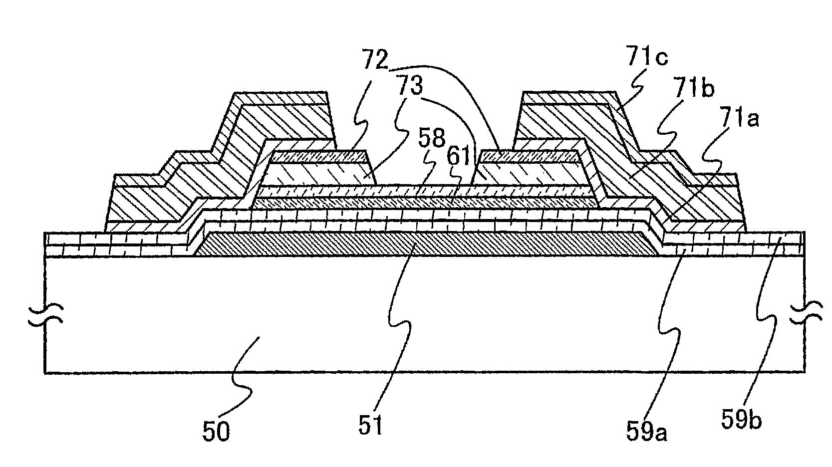
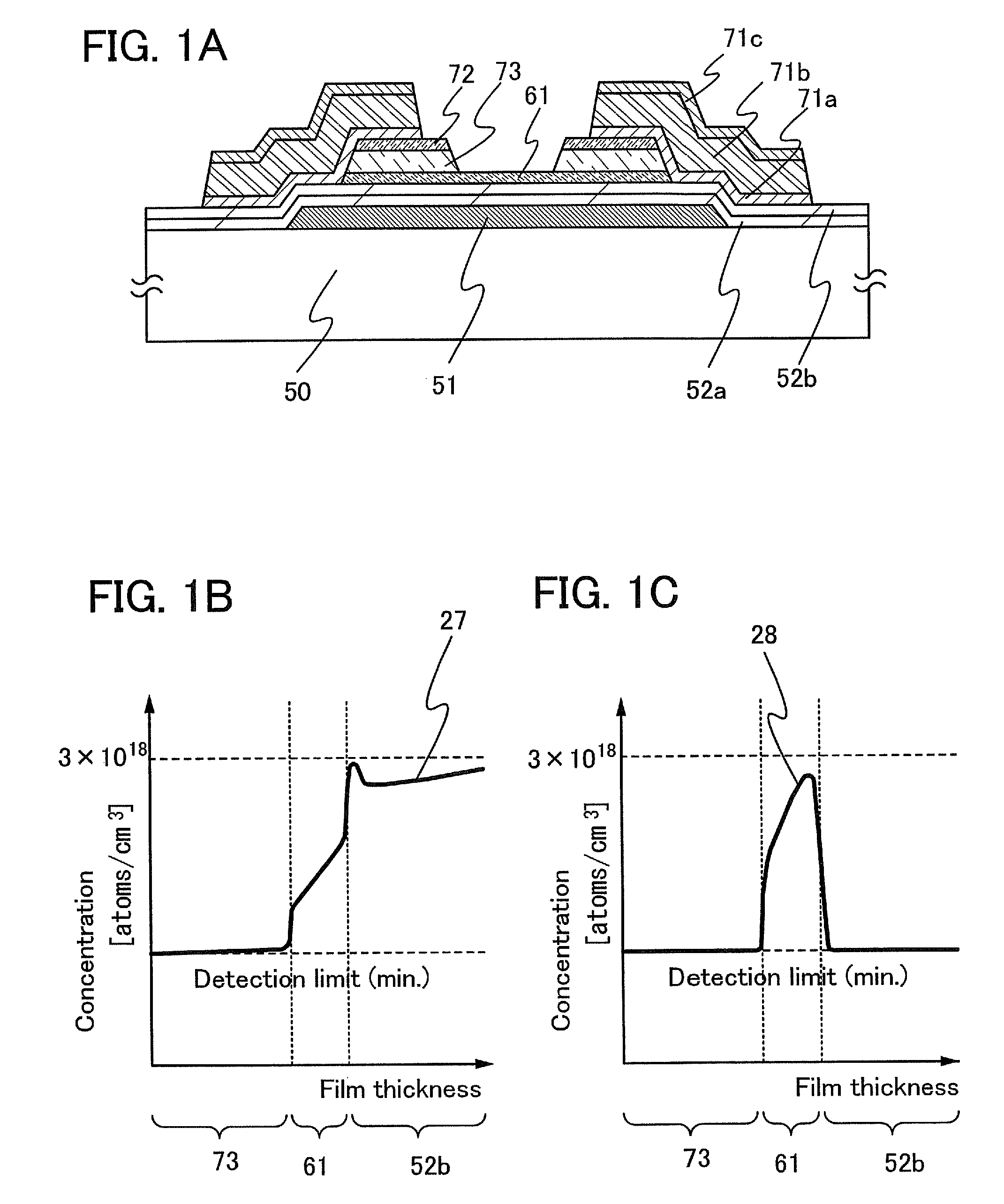
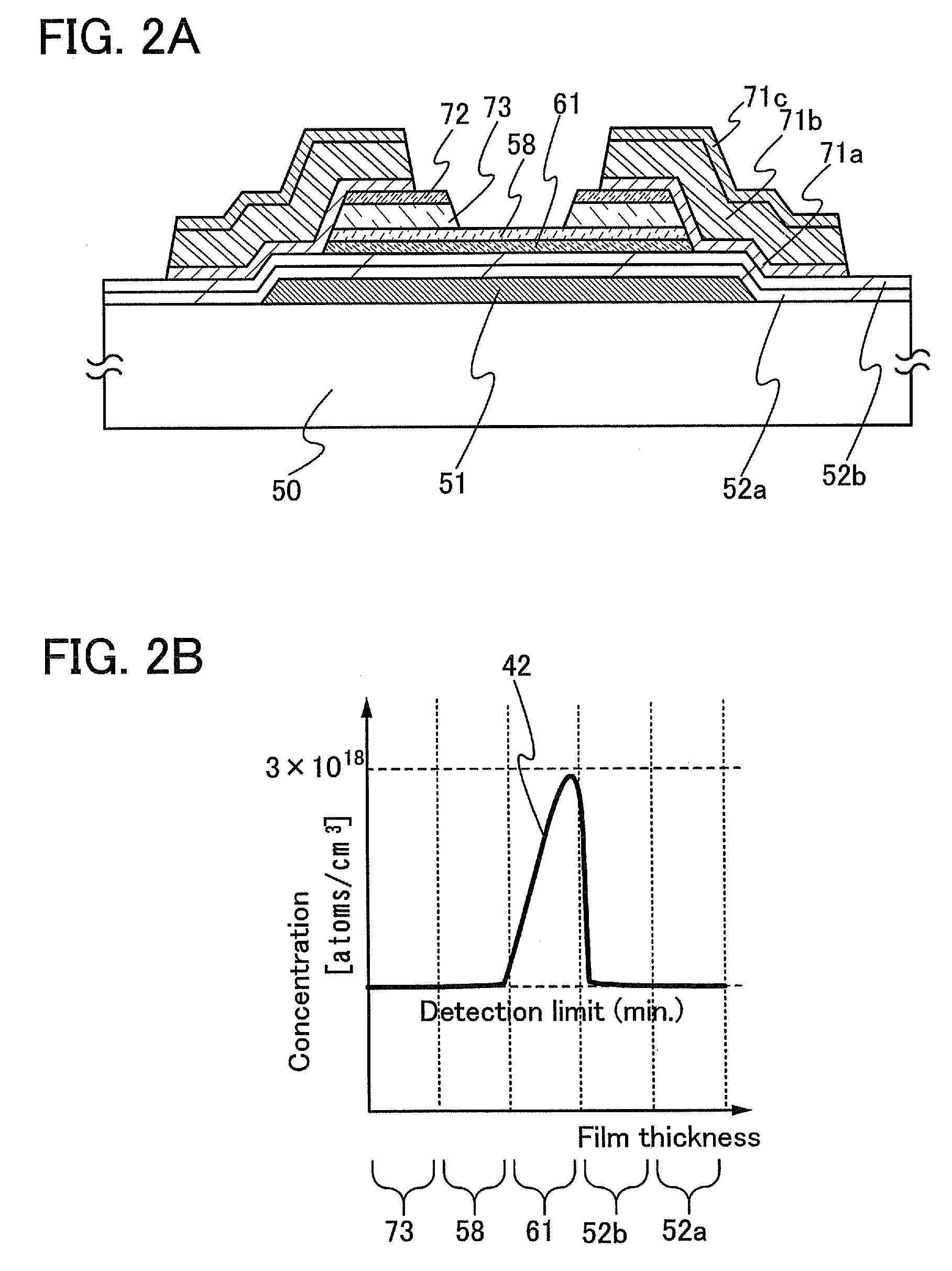
[0075]Now, a structure of a thin film transistor will be described with reference to FIGS. 1A to 1C. In the thin film transistor, crystallinity of an entire microcrystalline semiconductor film and at an interface between a gate insulating film and the microcrystalline semiconductor film is high, and the thin film transistor has a higher field effect mobility and higher on current than a thin film transistor having a conventional microcrystalline semiconductor film in a channel formation region.

[0076]In a thin film transistor shown in FIG. 1A, a gate electrode 51 is formed over a substrate 50, gate insulating films 52a and 52b are formed over the gate electrode 51, a microcrystalline semiconductor film 61 including an impurity element which serves as a donor is formed over the gate insulating films 52a and 52b, a pair of buffer layers 73 are formed over the microcrystalline semiconductor film 61, a pair of semiconductor films 72 to which an impurity element imparti...

embodiment mode 2

(Embodiment Mode 2)

[0126]In this embodiment mode, a method for forming a microcrystalline semiconductor film whose crystallinity in the entire film and at the interface with an insulating film is high will be described. Further, a process for manufacturing the thin film transistors described in Embodiment Mode 1 will be described, in which crystallinity of an entire microcrystalline semiconductor film and at the interface between a gate insulating film and the microcrystalline semiconductor film is high and of which field effect mobility and on current are higher than those of a thin film transistor including a conventional microcrystalline semiconductor film in a channel formation region.

[0127]A thin film transistor having a microcrystalline semiconductor film which is of an n-type is more suitable for use in a driver circuit than that of a p-type because the n-type thin film transistor has higher field effect mobility. It is preferable that all thin film transistors formed over th...

embodiment mode 3

(Embodiment Mode 3)

[0297]In this embodiment mode, a liquid crystal display device including the thin film transistor described in Embodiment Mode 1 or Embodiment Mode 2 will be described below as one mode of a display device. Here, a vertical alignment (VA) liquid crystal display device will be described with reference to FIG. 31, FIG. 32, and FIG. 33. The VA liquid crystal display device employs one mode for controlling alignment of liquid crystal molecules of a liquid crystal panel. The VA liquid crystal display device employs a mode in which liquid crystal molecules are vertical to a panel surface when voltage is not applied. In particular, in this embodiment mode, it is devised that a pixel is divided into several regions (sub-pixels) so that molecules are aligned in different directions in different regions. This is referred to as multi-domain or multi-domain design. In the following description, a liquid crystal display device with multi-domain design is described.

[0298]FIG. 3...


PUM


Abstract

The thin film transistor includes a gate insulating film formed over a gate electrode; a microcrystalline semiconductor film including an impurity element which serves as a donor, formed over the gate insulating film; a pair of buffer layers formed over the microcrystalline semiconductor film; a pair of semiconductor films to which an impurity element imparting one conductivity type is added, formed over the pair of buffer layers; and wirings formed over the pair of semiconductor films to which an impurity element imparting one conductivity type is added. The concentration of the impurity element which serves as a donor in the microcrystalline semiconductor film is decreased from the gate insulating film side toward the buffer layers, and the buffer layers do not include the impurity element which serves as a donor at a higher concentration than the detection limit of SIMS.

Description

BACKGROUND OF THE INVENTION[0001]1. Field of the Invention[0002]The present invention relates to a microcrystalline semiconductor film, a thin film transistor, and a display device including the thin film transistor at least in a pixel portion.[0003]2. Description of the Related Art[0004]In recent years, technology for forming thin film transistors using a thin semiconductor film (with a thickness of from several tens to several hundred of nanometers, approximately) formed over a substrate having an insulating surface has been attracting attention. Thin film transistors are applied in a wide range of electronic devices such as ICs or electro-optical devices, and development of thin film transistors that are to be used as switching elements in display devices, in particular, is being made actively.[0005]As a switching element in a display device, a thin film transistor including an amorphous semiconductor film, a thin film transistor including a polycrystalline semiconductor film, or...

Claims


Application Information

Patent Timeline
Patent Type & Authority Patents(United States)
IPC IPC(8): H01L29/76
CPCH01L29/04H01L29/4908H01L29/78696H01L29/78609H01L29/78678H01L29/66765
Inventor YAMAZAKI, SHUNPEIJINBO, YASUHIRO
Owner SEMICON ENERGY LAB CO LTD
Why Eureka
Try Eureka