

DSP block for implementing large multiplier on a programmable integrated circuit device
a technology of programmable integrated circuits and multipliers, applied in the field of programmable integrated circuit devices, can solve the problems of increasing complexity of applications for which plds are used, slow and less efficient, and consuming general-purpose resources that might be put to other uses, so as to reduce or eliminate the reliance on general-purpose programmable resources and the effect of large operations
- Summary
- Abstract
- Description
- Claims
- Application Information
AI Technical Summary
Benefits of technology
Problems solved by technology
Method used
Image

Examples
Embodiment Construction
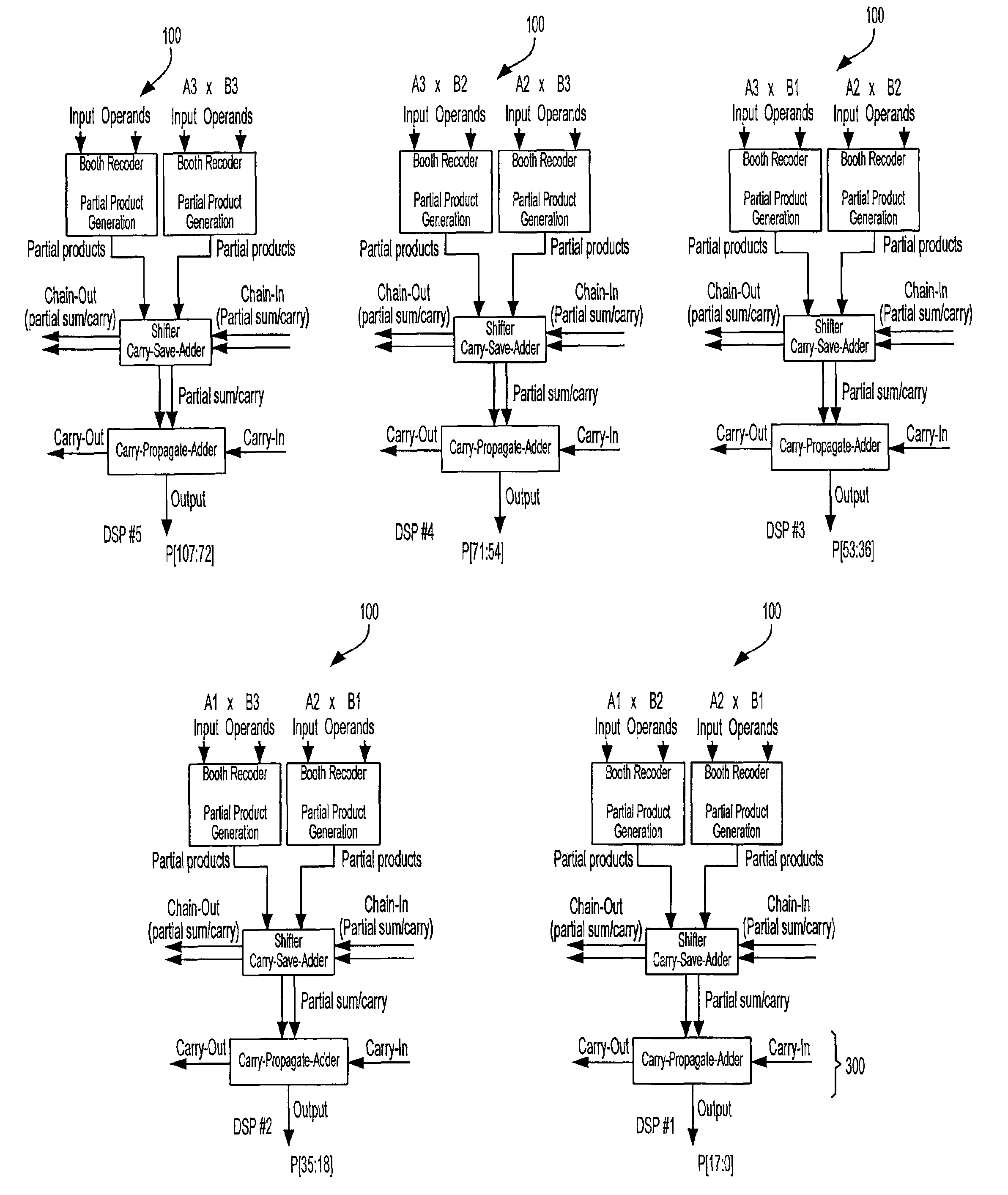
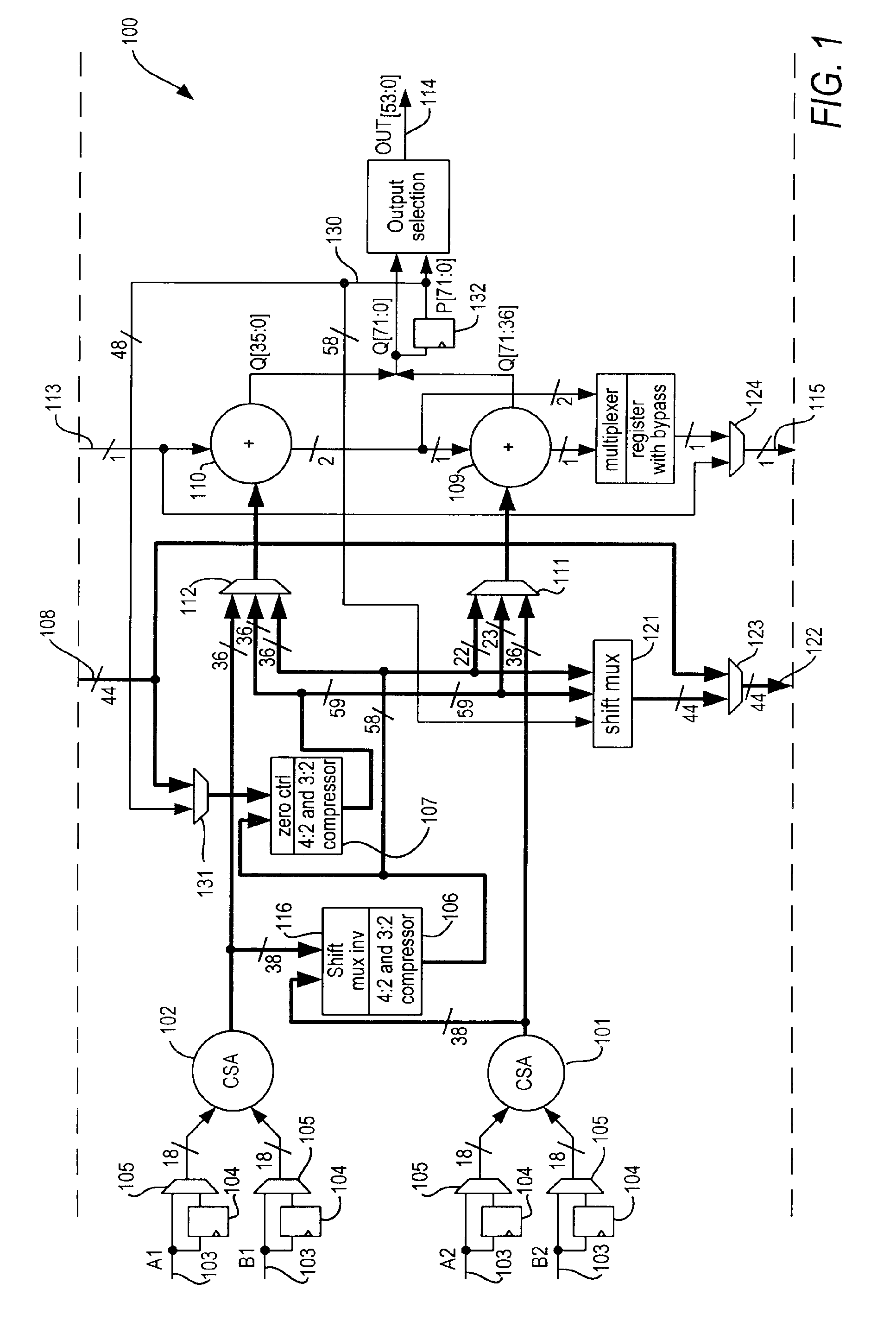
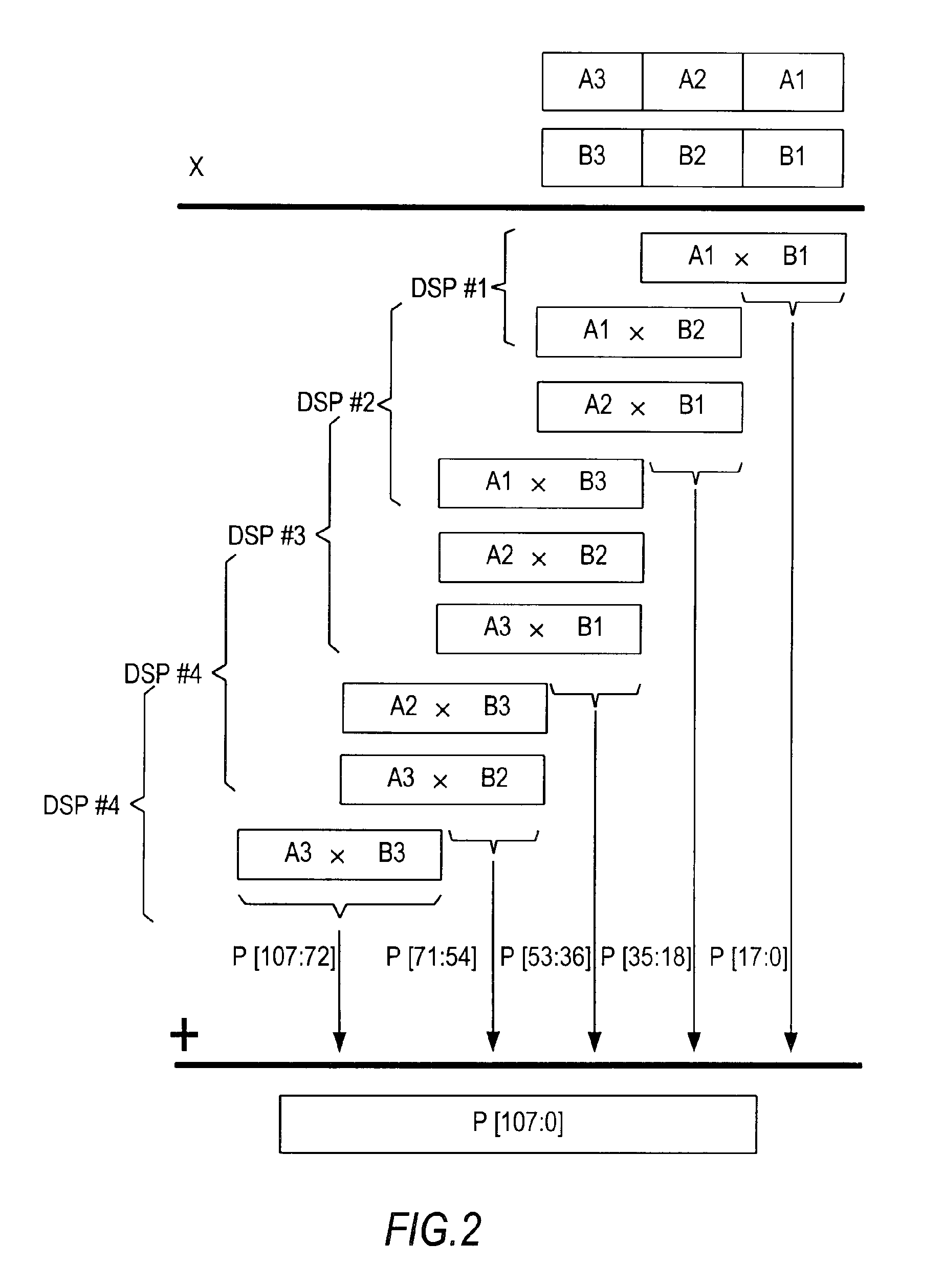
[0017]A DSP block in accordance with the present invention may include one or more N-bit-by-N-bit multipliers. Such a DSP block may include the following functional blocks:[0018]1. Partial product generation, preferably based on Booth recoding;[0019]2. A respective carry-save adder for partial products from each multiplier;[0020]3. A further carry-save adder for partial sum / carry from all multipliers within the DSP block, as well as the chained-in partial sum / carry from any adjacent DSP block; and[0021]4. A carry-propagate adder for the final output.
[0022]Such a DSP architecture provides the logic to generate partial sum / carry from multipliers of the aforementioned relatively small operand sizes, and to add the partial sum / carry from the current DSP block and an adjacent DSP block. Because the chain-in from any adjacent DSP block is based on partial sum / carry signals from a carry-save adder, the propagation delay to add the chain-in results is that contributed by one 4-to-2 compress...
PUM
 Abstract
Description
Claims
Application Information