Large multiplier for programmable logic device

a programmable logic and multiplier technology, applied in the field of programmable logic devices, can solve the problems of increasing complexity of applications for which plds are used, consuming general-purpose resources that might be put to other uses, slow and less efficient, etc., and achieves the effect of reducing or eliminating the reliance on general-purpose programmable resources and facilitating the performance of multiplication

Active Publication Date: 2008-06-05
ALTERA CORP
View PDF99 Cites 73 Cited by
  • Summary
  • Abstract
  • Description
  • Claims
  • Application Information

AI Technical Summary

Benefits of technology

[0006]The present invention relates to specialized processing blocks for PLDs that are provided with logic within the blocks to facilitate the performance of multiplications larger than that which can be performed within any single specialized processing block, reducing or eliminating reliance on general-purpose programmable resources of the PLD.

Problems solved by technology

As applications for which PLDs are used increase in complexity, it has become more common to design PLDs to include specialized processing blocks in addition to blocks of generic programmable logic resources.
While the multipliers from several DSP blocks can be used together to implement double-precision multiplication, the logic needed to interconnect the multipliers has heretofore been programmed by the user in the general-purpose programmable logic outside the DSP block, making it slow and less efficient, and consuming general-purpose resources that might be put to other uses.

Method used


Image

  • Large multiplier for programmable logic device
  • Large multiplier for programmable logic device
  • Large multiplier for programmable logic device

Examples


Embodiment Construction

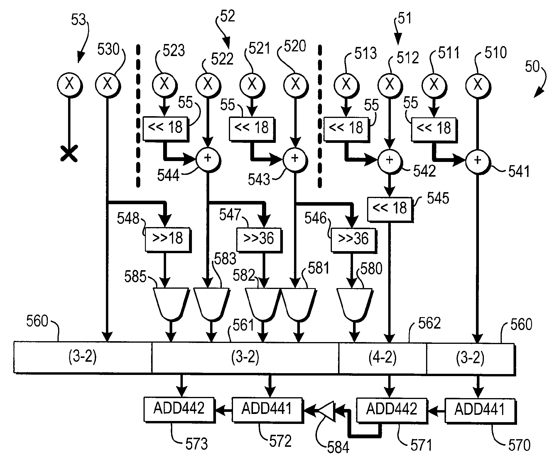
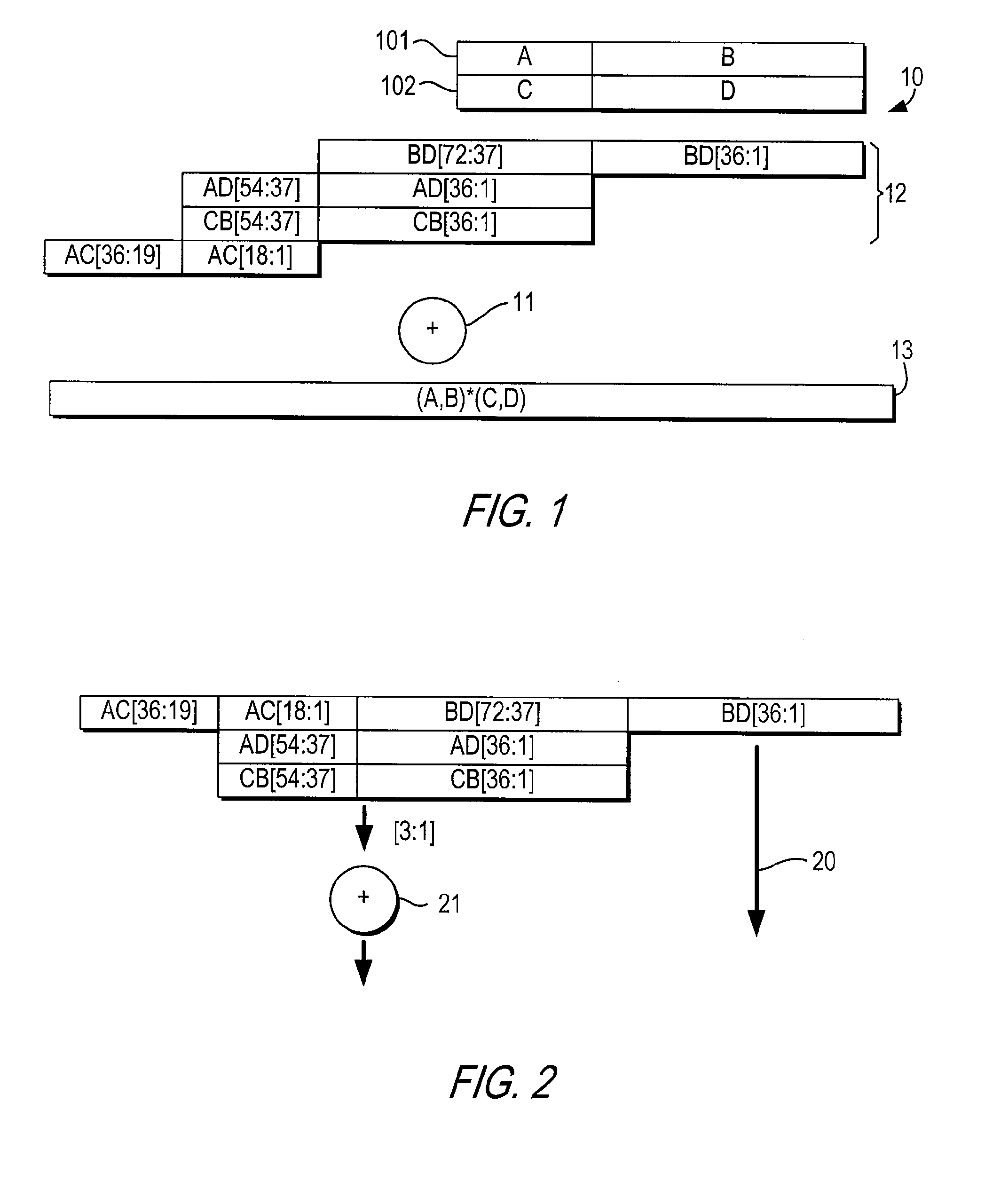
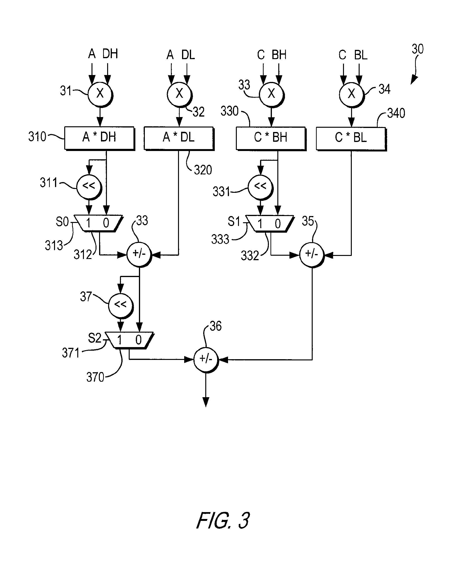
[0020]The invention will now be described with reference to FIGS. 1-6, in the context of a 54-bit-by-54-bit multiplication, which maps well onto the 18-bit multipliers of the DSP block of the aforementioned STRATIX® II PLD, and which can be used to implement double-precision multiplication under the IEEE 754-1985 standard. However, the invention can be used with specialized processing blocks of different sizes.

[0021]FIG. 1 shows the decomposition of a 54-bit-by-54-bit multiplication 10 into a sum 11 of partial products 12 that can be implemented using 18-bit-by-18-bit multipliers to yield product 13. In the first multiplicand 101, A contains the 18 most significant bits, and B contains the 36 least significant bits. In the second multiplicand 102, C contains the 18 most significant bits, and C contains the 36 least significant bits. The result (A,B)×(C,D) can be calculated as B×D+((A×D+C×B)<<36)+((A×C)<<72), where “<


PUM


Abstract

A plurality of specialized processing blocks in a programmable logic device, including multipliers and circuitry for adding results of those multipliers, can be configured as a larger multiplier by adding to the specialized processing blocks selectable circuitry for shifting multiplier results before adding. In one embodiment, this allows all but the final addition to take place in specialized processing blocks, with the final addition occurring in programmable logic. In another embodiment, additional compression and adding circuitry allows even the final addition to occur in the specialized processing blocks.

Description

BACKGROUND OF THE INVENTION [0001]This invention relates to programmable logic devices (PLDs), and, more particularly, to the use of specialized processing blocks which may be included in such devices to perform large multiplications.[0002]As applications for which PLDs are used increase in complexity, it has become more common to design PLDs to include specialized processing blocks in addition to blocks of generic programmable logic resources. Such specialized processing blocks may include a concentration of circuitry on a PLD that has been partly or fully hardwired to perform one or more specific tasks, such as a logical or a mathematical operation. A specialized processing block may also contain one or more specialized structures, such as an array of configurable memory elements. Examples of structures that are commonly implemented in such specialized processing blocks include: multipliers, arithmetic logic units (ALUs), barrel-shifters, various memory elements (such as FIFO / LIFO...

Claims


Application Information

Patent Timeline
Patent Type & Authority Applications(United States)
IPC IPC(8): G06F7/57G06F17/00
CPCG06F7/52G06F7/5324
Inventor LANGHAMMER, MARTINTHARMALINGAM, KUMARA
Owner ALTERA CORP
Why Eureka
Try Eureka