LED module and LED lamp having the LED module

a technology of led modules and led lamps, which is applied in the direction of point-like light sources, semiconductor devices of light sources, lighting and heating apparatus, etc., can solve the problems of increasing power and increasing the resulting generated heat, and achieves the effects of enhancing the heat dissipation effect, simplifying the package process, and reducing the thermal resistance layer

Active Publication Date: 2012-11-13
LITE ON ELECTRONICS (GUANGZHOU) LTD +1
View PDF6 Cites 1 Cited by
  • Summary
  • Abstract
  • Description
  • Claims
  • Application Information

AI Technical Summary

Benefits of technology

[0007]Therefore, an object of the present invention is to provide a multi-chip LED module that can simultaneously use horizontal and vertical types of chips, that has flexibility for circuit design, and that can enhance the effect of heat dissipation.
[0009]The efficiency of the LED module of the present invention resides in the fact that through the patterned conductive layer which has a plurality of die-bonding pads, flexibility is provided with respect to the use of the circuit design and the chip type. Further, the dielectric layer and the patterned conductive layer may respectively be a ceramic layer and a copper layer that are soldered to form a multi-layered structure. The LED chip may be directly connected to the patterned conductive layer (Chip-on-Board) to thereby minimize the thermal resistant layers and enhance the effect of heat dissipation. Moreover, the LED module has a chip-receiving hole and a surrounding structure or a ring structure, and can simplify a package process.

Problems solved by technology

Technological progress in producing light emitting diode (LED) chips has resulted in an increase in the power of the LED chips, and this, in turn, has resulted in an increase in the resulting generated heat.

Method used


Image

  • LED module and LED lamp having the LED module
  • LED module and LED lamp having the LED module
  • LED module and LED lamp having the LED module

Examples


Embodiment Construction

[0032]The above-mentioned and other technical contents, features, and effects of this invention will be clearly presented from the following detailed description of five preferred embodiments in coordination with the reference drawings.

[0033]Before this invention is described in detail, it should be noted that, in the following description, similar elements are designated by the same reference numerals.

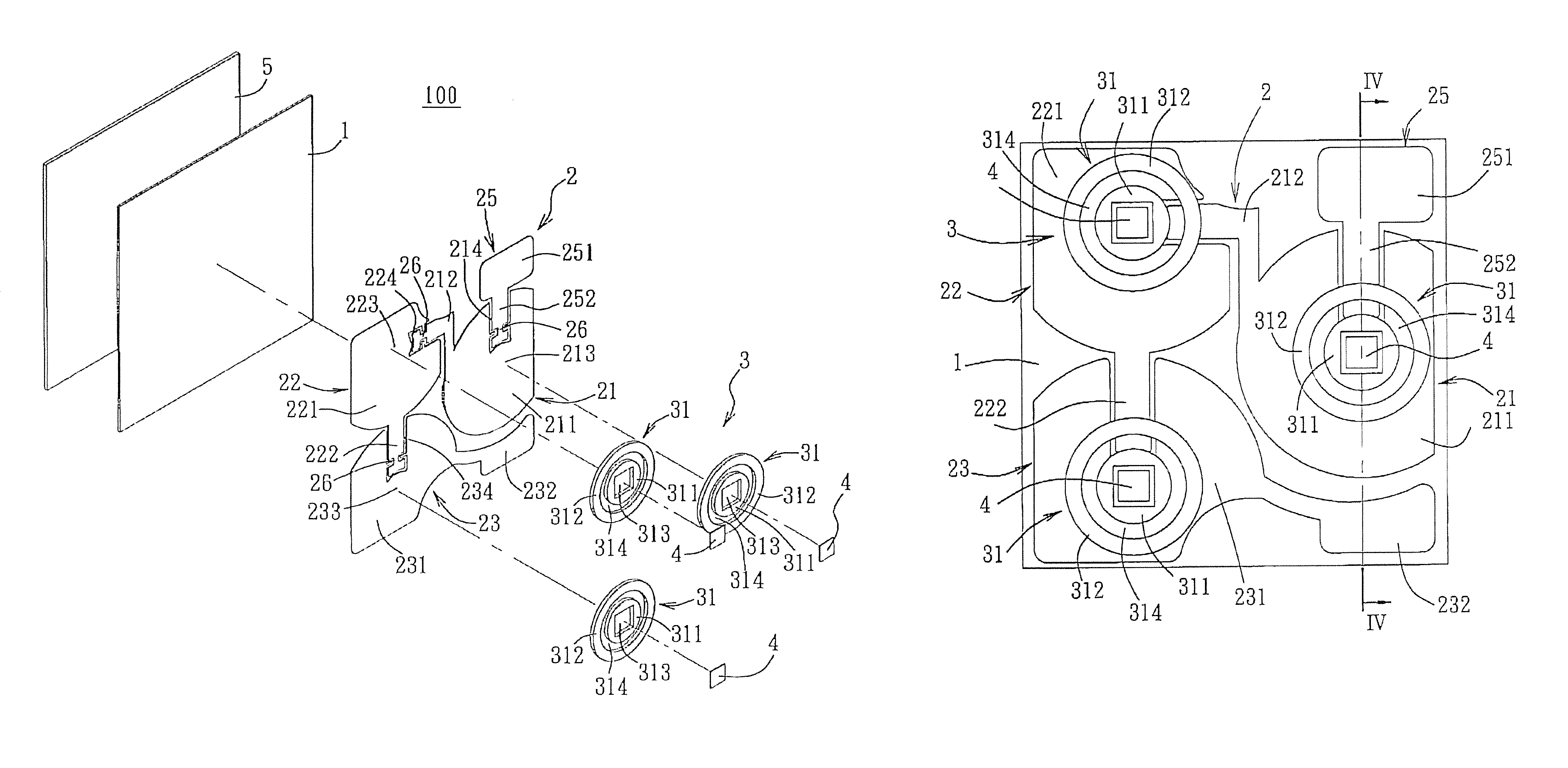
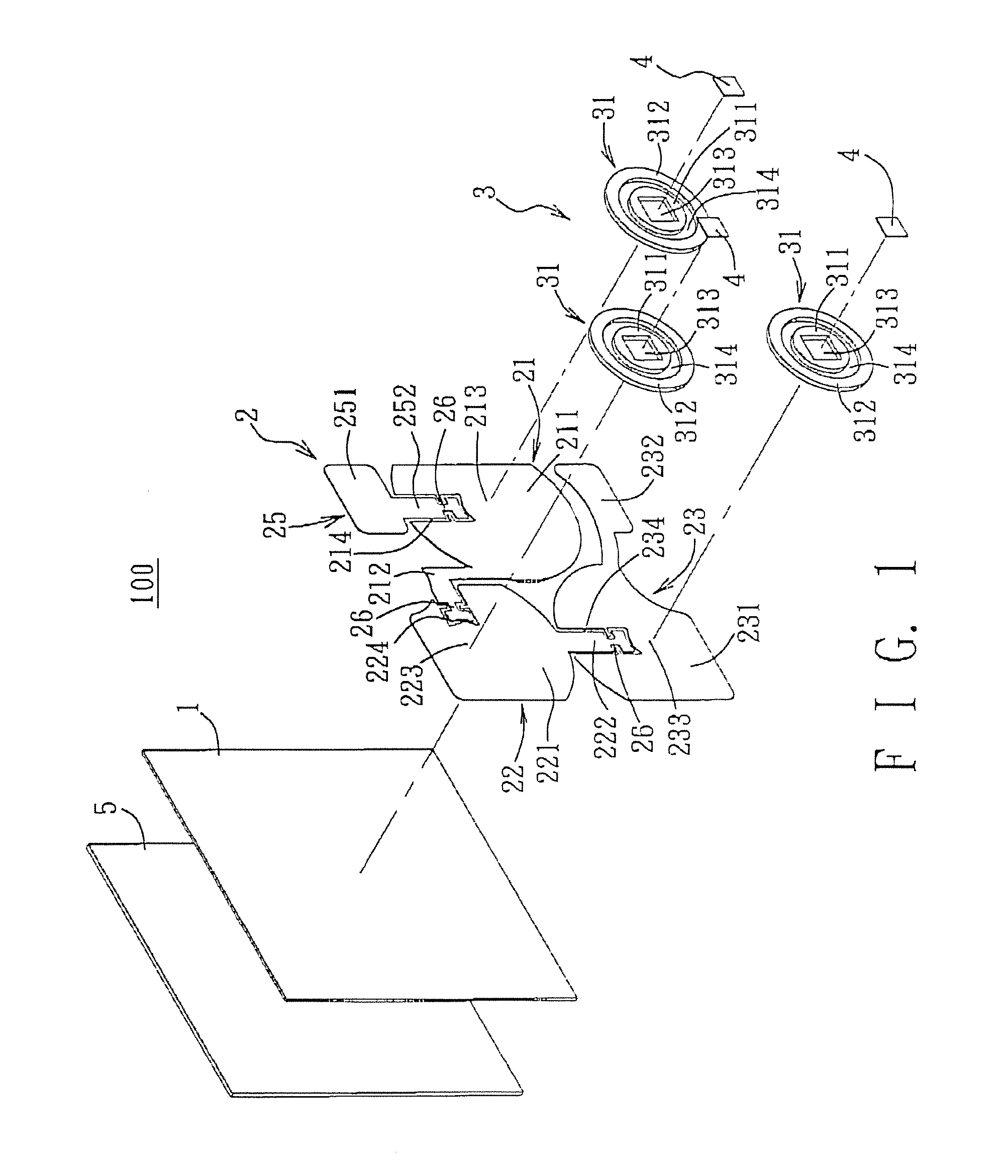
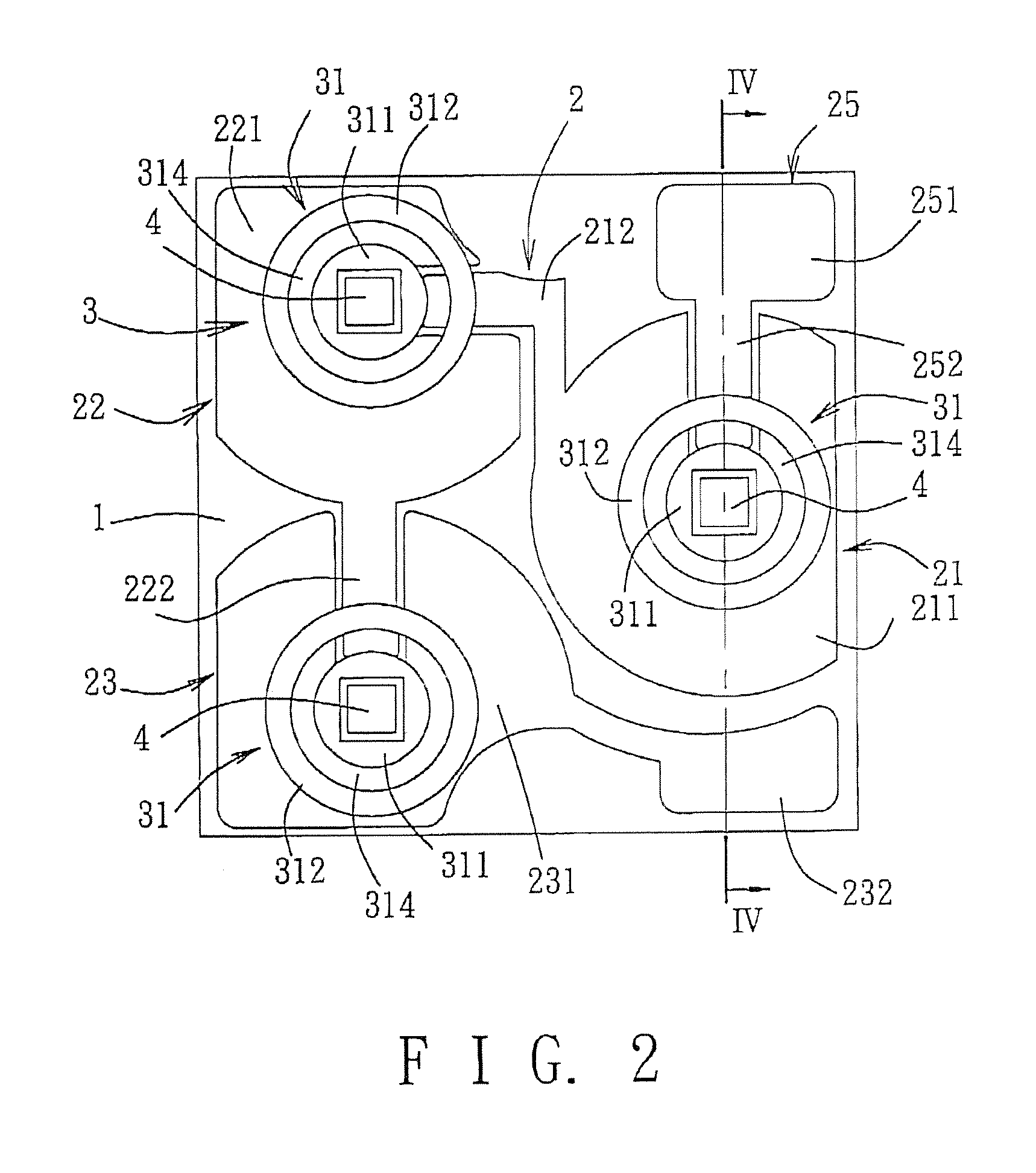
[0034]Referring to FIGS. 1 to 3, an LED module 100 according to the first preferred embodiment of the present invention comprises a first dielectric layer 1, a first patterned conductive layer 2, a second dielectric layer 3, three LED chips 4, and a metallic layer 5 disposed below the first dielectric layer 1.

[0035]The first patterned conductive layer 2 is disposed on the first dielectric layer 1, and includes three die-bonding pads 21, 22, 23 arranged in a substantially triangular fashion. The arrangement is such that the first die-bonding pad 21 is located on the right side, the sec...


PUM


Abstract

An LED module includes a first dielectric layer, and a first patterned conductive layer having first, second, and third die-bonding pads. Each die-bonding pad includes a pad body having a die-bonding area, and an extension extended from the pad body. The extension of the first die-bonding pad extends in proximity to the die-bonding area of the second die-bonding pad. The extension of the second die-bonding pad extends in proximity to the die-bonding area of the third die-bonding pad. A second dielectric layer disposed on the first patterned conductive layer includes three dielectric members corresponding respectively to the die-bonding pads of the first patterned conductive layer. Each dielectric member includes a chip-receiving hole exposing the die-bonding area of a respective die-bonding pad for attachment of an LED chip thereto, and a wire-passage hole spaced apart from the chip-receiving hole to expose partially the first patterned conductive layer for bonding a wire.

Description

CROSS-REFERENCE TO RELATED APPLICATION[0001]This application claims priority of Chinese Application No. 201010170011.6, filed on May 4, 2010.BACKGROUND OF THE INVENTION[0002]1. Field of the Invention[0003]This invention relates to a light emitting diode (LED) module, more particularly to a light emitting diode (LED) module with a chip-on-board (COB) structure and including at least two LED chips and a light emitting diode (LED) lamp having the LED module.[0004]2. Description of the Related Art[0005]Technological progress in producing light emitting diode (LED) chips has resulted in an increase in the power of the LED chips, and this, in turn, has resulted in an increase in the resulting generated heat. As a consequence, the heat-dissipating effect of an LED package structure becomes an important factor that affects the quality of an LED product. Hence, there are continuous efforts to enhance the heat-dissipating effect of LED package structures. Currently, a package body having a pl...

Claims


Application Information

Patent Timeline
Patent Type & Authority Patents(United States)
IPC IPC(8): H01L29/18
CPCF21K9/10H05K1/0295H01L25/0753H01L33/62H05K1/0207H05K2201/10106H05K2203/049F21Y2101/02H01L2224/48091H01L2924/00014H01L2224/49175H01L2224/8592H01L2924/00H01L2924/19107F21K9/20F21Y2115/10
Inventor LIANG, CHIH-LUNGWANG, YAN-YU
Owner LITE ON ELECTRONICS (GUANGZHOU) LTD
Why Eureka
Try Eureka