Variable ring width SDD

a ring width and variable technology, applied in the field ofsilicon drift detectors, can solve the problems of large capacitance, poor resolution, and high manufacturing cost of sdds with electrically coupled rings, and achieve the effects of reducing manufacturing cost, reducing capacitance, and reducing manufacturing cos

Inactive Publication Date: 2012-11-20
MOXTEK INC
View PDF17 Cites 3 Cited by
  • Summary
  • Abstract
  • Description
  • Claims
  • Application Information

AI Technical Summary

Benefits of technology

[0009]It has been recognized that it would be advantageous to create a radiation detector having a small anode area for reduced capacitance. It has been recognized that it would be advantageous to create a radiation detector that is relatively less expensive to manufacture.
[0010]The present invention is a silicon drift detector comprised of a substrate with a first conduction type. The substrate includes a top surface and a bottom surface. A layer, having a second conduction type, is disposed at the bottom surface of the substrate. An island region having the first conduction type is disposed at the top surface of the substrate. At least two rings can be disposed at the top surface of the substrate and substantially circumscribe the island region. The rings are electrically isolated from each other. Due to the lack of electrical coupling between the rings, the manufacturing cost can be reduced. This invention includes a relatively small anode for reduced capacitance.

Problems solved by technology

A disadvantage of the PIN diode is the large capacitance due to the large anode size.
Such capacitance can result in undesirable electronic noise, resulting in poor resolution.
Although the prior art SDDs can have reduced electronic noise compared with the prior art PIN diode, such SDDs with electrically coupled rings can be costly to manufacture.

Method used


Image

  • Variable ring width SDD
  • Variable ring width SDD
  • Variable ring width SDD

Examples


Embodiment Construction

[0023]Reference will now be made to the exemplary embodiments illustrated in the drawings, and specific language will be used herein to describe the same. It will nevertheless be understood that no limitation of the scope of the invention is thereby intended. Alterations and further modifications of the inventive features illustrated herein, and additional applications of the principles of the inventions as illustrated herein, which would occur to one skilled in the relevant art and having possession of this disclosure, are to be considered within the scope of the invention.

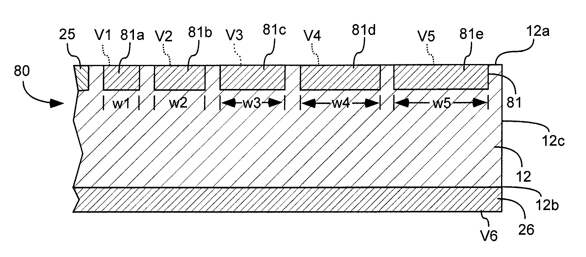
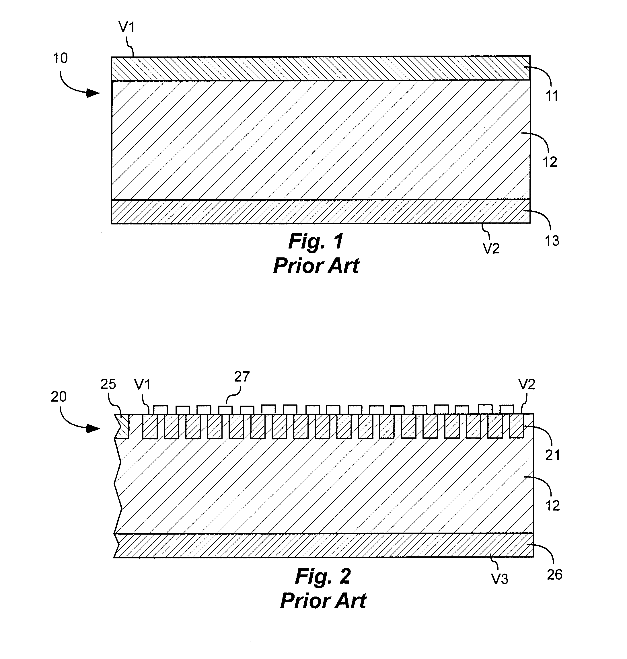
[0024]Referring to FIG. 5, a silicon drift detector (SDD), indicated generally at 50, in accordance with an exemplary embodiment is shown. The SDD includes a substrate 12 having a first conduction type, and with top and bottom surface. The top and bottom surfaces are opposite one another and can be oriented in any direction. A layer 26 (FIGS. 7-9) having a second conduction type can be disposed at the bottom surf...


PUM


Abstract

A silicon drift detector (SDD) comprising electrically isolated rings. The rings can be individually biased doped rings. One embodiment includes an SDD with a single doped ring. Some of the doped rings may not require a bias voltage. Some of the rings can be field plate rings. The field plate rings may all use the same biasing voltage as a single outer doped ring. The ring widths can vary such that the outermost ring is widest and the ring widths decrease with each subsequent ring towards the anode.

Description

CLAIM OF PRIORITY[0001]This is a continuation-in-part of U.S. patent application Ser. No. 12 / 575,939, filed on Oct. 8, 2009; which claims priority of Japan Patent Application Serial No. 2009-157627, filed Jul. 2, 2009; and which claims priority to U.S. Patent Application Ser. Nos. 61 / 185,679 and 61 / 185,754, both filed Jun. 10, 2009; which are hereby incorporated herein by reference in their entirety.FIELD OF THE INVENTION[0002]The present invention relates to silicon drift detectors.BACKGROUND[0003]Various types of radiation detectors, such as silicon PIN diode detectors or silicon drift detectors, are used for measuring the energy of incoming x-ray photons. A PIN diode can be used for collecting charge carriers that are proportional in number to the energy of the x-ray photon. An example of a PIN diode is illustrated in FIG. 1, shown generally at 10. The PIN diode is comprised of a substrate 12, often referred to as an intrinsic region, an anode 11 on one surface of the substrate, ...

Claims


Application Information

Patent Timeline
Patent Type & Authority Patents(United States)
IPC IPC(8): H01L31/115
CPCG01T1/2928H01L31/115
Inventor HULLINGER, DEREKMATSUURA, HIDEHARUTANIGUCHI, KAZUOUTAKA, TADASHI
Owner MOXTEK INC
Why Eureka
Try Eureka