Method for handling a semiconductor wafer assembly

a technology of semiconductor wafers and wafer assemblies, which is applied in the direction of semiconductor devices, basic electric elements, electrical apparatus, etc., can solve the problems of obstructing light, reducing obstructing light, so as to reduce the area of light emitting from the device, reduce the effect of light, and increase the led performan

Active Publication Date: 2012-11-27
SEMILEDS OPTOELECTRONICS CO LTD
View PDF9 Cites 21 Cited by
  • Summary
  • Abstract
  • Description
  • Claims
  • Application Information

AI Technical Summary

Benefits of technology

[0030]Advantage of the invention may include one or more of the following. No wafer bonding or gluing is used and the complex and lengthy and one at a time wafer bonding / gluing process is replaced by a less complex deposition process for example physical vapor deposition (PVD), chemical vapor deposition (CVD), plasma enhanced CVD (PECVD), evaporation, ion beam deposition, electro chemical deposition, electroless chemical deposition, plasma spray, or ink jet deposition. No semi-transparent contact is needed for the n-electrode since n-GaN conductivity is good, and as a result, more light output can be emitted from the LED device. Further, since only one electrode is needed on each side of the device, the LED electrode obstructs less light. Additionally, current can spread out uniformly from n-electrode to p-electrode, thus increasing LED performance. Moreover, the metal substrate can dissipate more heat than the sapphire substrate, so more current can be used to drive the LED. The resulting LED can replace the conventional LED at a smaller size. For the same LED size, the light output from vertical LED is significantly higher than the conventional LED for the same drive current. Moreover, the multi-layered metal substrate may be engineered by designing the thickness and composition of the individual metal layers to prevent cracking of the GaN device structure and achieve a desired hardness and thermal expansion coefficient.
[0031]Yet another embodiment of the present invention is a method. The method generally includes the steps of providing a wafer assembly comprising one or more semiconductor dies disposed on a carrier substrate; forming one or more metal layers above the one or more semiconductor dies to create at least a portion of a metal substrate; removing the carrier substrate from the wafer assembly; and manipulating the wafer assembly via the metal substrate for further processing. The thickness and composition of the layers of a multi-layered metal substrate may be designed to minimize cracking of the semiconductor dies at elevated temperatures during subsequent operations.
[0032]Yet another embodiment of the present invention is a method. The method generally includes the steps of providing a wafer assembly comprising one or more vertical light-emitting diode (VLED) dies disposed on a carrier substrate; forming one or more metal layers above the one or more VLED dies to create at least a portion of a metal substrate; removing the carrier substrate from the wafer assembly; and handling the wafer assembly via the metal substrate for further semiconductor processing. The thickness and composition of the layers of a multi-layered metal substrate may be designed to minimize cracking of the VLED dies at elevated temperatures during subsequent operations.

Problems solved by technology

However such configuration of electrodes and electrically non-conductive nature of sapphire substrate represents a significant limitation for the device operation.
Moreover, p- and n-electrodes obstruct the light and reduce the area of light emitting from the device.
Additionally, the sapphire substrate is a heat insulator (or a thermal insulator) and the heat generated during the device operation can not be effectively dissipated, thus limiting the device reliability.
However, limitations of this conventional LED structure include: (1) Semi-transparent contact on p-layer 5 is not 100% transparent and can block the light emitted from layer 4; (2) current spreading from n-electrode to p-electrode is not uniform due to position of electrodes; and (3) heat is accumulated during device operation since sapphire is a thermal and electrical insulator.

Method used


Image

  • Method for handling a semiconductor wafer assembly
  • Method for handling a semiconductor wafer assembly
  • Method for handling a semiconductor wafer assembly

Examples


Embodiment Construction

[0038]In reading the detailed description, the accompanying drawings may be referenced at the same time and considered as part of the detailed description.

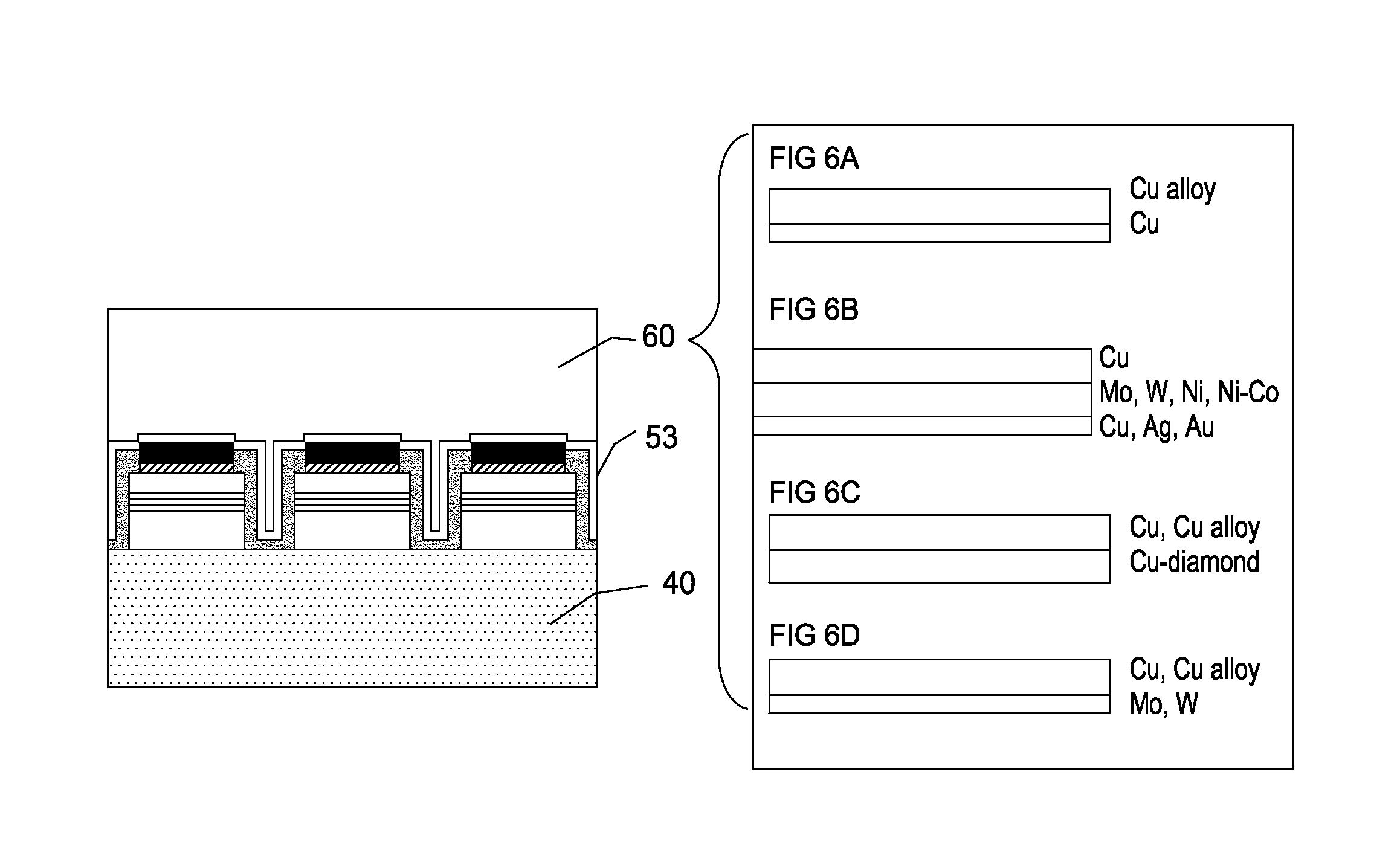
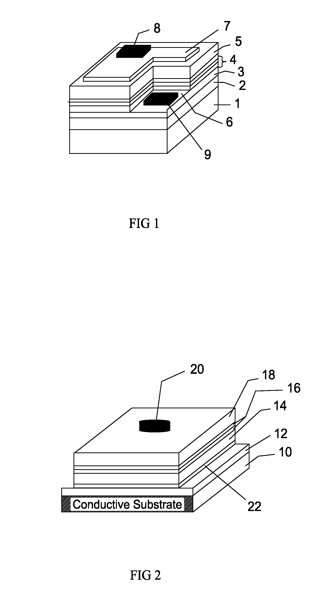
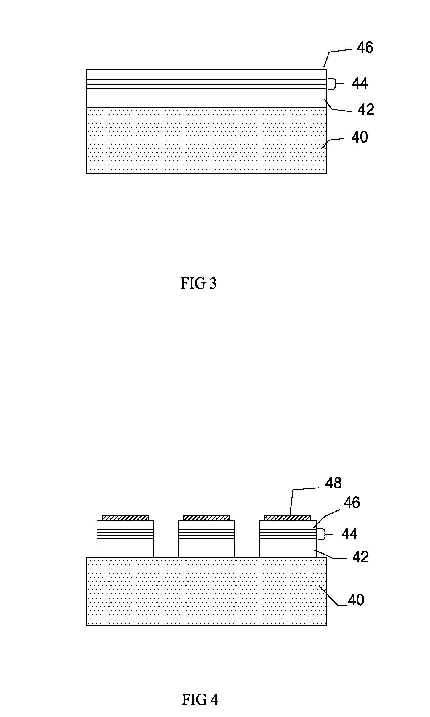
[0039]Referring to FIGS. 3 to 8, a manufacturing method for vertical LEDs is illustrated therein. In the description, the reference numerals given for the inventive device structure will be also used in the recitation of the steps of the inventive manufacturing method.

[0040]The process described below is for one embodiment with InGaN LEDs initially grown on sapphire. Electro or Electroless Chemical plating is then used to deposit a thick contact for electrical and thermal conduction for the resulting LED device. Electro or Electroless Chemical plating is used in lieu of wafer bonding. The process can be applied to any optoelectronic device where bonding was used to attach the epilayer to a new host substrate for improvement of optical, electrical and thermal properties.

[0041]For example, the techniques described herein may be appl...


PUM


Abstract

Systems and methods for fabricating a light emitting diode include forming a multilayer epitaxial structure above a carrier substrate; depositing at least one metal layer above the multilayer epitaxial structure; removing the carrier substrate.

Description

CROSS-REFERENCE TO RELATED APPLICATIONS[0001]This application is a continuation-in-part of U.S. patent application Ser. No. 11 / 032,882, filed Jan. 11, 2005, now U.S. Pat. No. 7,432,119 which is herein incorporated by reference.BACKGROUND OF THE INVENTION[0002]1. Field of the Invention[0003]The present invention generally relates to a light-emitting diode and a method for fabricating the same.[0004]2. Description of the Related Art[0005]Light-emitting diodes (LEDs) are playing an increasingly important role in our daily life. Traditionally, LEDs are become ubiquitous in many applications, such as communications and other areas, such as mobile phones, appliances and other electronic devices. Recently, the demand for nitride based semiconductor materials (e.g., having Gallium Nitride or GaN) for opto-electronics has increased dramatically for applications such as video displays, optical storage, lighting, medical instruments, for-example. Conventional blue light-emitting diodes (LEDs) ...

Claims


Application Information

Patent Timeline
Patent Type & Authority Patents(United States)
IPC IPC(8): H01L21/20
CPCH01L33/0079H01L33/0093H01L21/00H01L21/20
Inventor DOAN, TRUNG TRICHU, CHEN-FU
Owner SEMILEDS OPTOELECTRONICS CO LTD
Why Eureka
Try Eureka