Display device and a method of driving the same

a technology of a display device and a drive mechanism, which is applied in the direction of static indicating devices, instruments, sustainable buildings, etc., can solve the problems of limiting the disposition portion, unable to dispose of the conductive film for the touch panel, and difficult to realistically apply the liquid crystal element with the touch panel to an application of the mobile devi

Active Publication Date: 2012-11-27
JAPAN DISPLAY WEST
View PDF5 Cites 26 Cited by
  • Summary
  • Abstract
  • Description
  • Claims
  • Application Information

AI Technical Summary

Benefits of technology

[0012]In this case, the A.C. drive scanning portion carries out the A.C. driving operation while changing a combination (the objects of the selection) of two or more counter electrodes simultaneously driven. At this time, the A.C. drive scanning portion carries out the shifting operation so that the common one or more counter electrodes are contained in the objects of the selection with the continuous two A.C. driving operations. Therefore, a step of the shift of the group of counter electrodes which are being A.C. driven is smaller than that of the step of the shift of the group of counter electrodes which are being simultaneously A.C. driven. To put it the other way around, a width of the group of counter electrodes which are being simultaneously A.C. driven can be made large although the counter electrodes are finely shifted. Therefore, contradictory two operations, that is, the reducing of the step of the shift of the counter electrodes, and the reducing of the effective division number of counter electrodes are compatible with each other.
[0016]According to the embodiments of the present invention, it is possible to provide the display device which has the configuration allowing the display device to be thinned, and which carries out the driving operation adapted to the configuration, and the method of driving the same.

Problems solved by technology

Therefore, setting aside the question of a stationary television receiver powered through a socket, it is difficult to realistically apply the liquid crystal element with the touch panel to an application of the mobile device.
In addition, in the technique described above, since it is necessary for the conductive film for the touch panel to be very close to the finger of the user, it is impossible to dispose the conductive film for the touch panel, for example, in a deeper portion of the liquid crystal display element, and so forth.
As a result, there is a limit to a disposition portion.
Thus, it is difficult to integrate the circuits in terms of the entire device.

Method used


Image

  • Display device and a method of driving the same
  • Display device and a method of driving the same
  • Display device and a method of driving the same

Examples


first embodiment

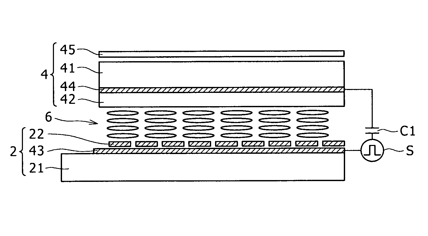
[0048]FIGS. 4A to 4C respectively show top plan views specialized in dispositions of electrodes, and a circuit or driving or detecting the electrode in the display device according to the first embodiment. Also, FIG. 4D shows a schematic cross sectional view of a structure of the display device according to the first embodiment. FIG. 4D shows a cross section for six pixels, for example, in a row direction (in a pixel display line direction). FIG. 5 is an equivalent circuit diagram of a pixel. The display device illustrated in FIGS. 4A to 4D is a liquid crystal display device including a liquid crystal layer as “a display functional layer.”

[0049]The liquid crystal display device 1, as previously stated, has an electrode (counter electrode). In this case, this counter electrode is a common electrode, common to a plurality of pixels, of two electrodes facing to each other so as to hold the liquid crystal layer between them. Also, a common drive signal Vcom giving a signal voltage for g...

second embodiment

[0086]Next, a second embodiment of the present invention will be described in detail with reference to FIG. 10, FIGS. 11A and 11B, and FIGS. 12A and 12B. In the second embodiment, unlike the case of the first embodiment described above, a liquid crystal element having a transverse electric field mode is used as the display element.

[0087]FIG. 10 is a schematic cross sectional view showing a structure of the liquid crystal display device according to the second embodiment of the present invention. In FIG. 10, portions corresponding to those in the first embodiment are designated with the same reference numerals, respectively, and a description thereof is suitably omitted here for the sake of simplicity.

[0088]The display device of the second embodiment is different exclusively to positions of the electrodes (having the different patterns) from the display device of the first embodiment in that the counter electrodes 43 are disposed on the drive substrate 2 side. The counter electrodes ...

third embodiment

[0098]A third embodiment provides another driving method which can be applied to the liquid crystal display device having any of the structures of the first and second embodiments described above.

[0099]FIG. 14 shows a method of A.C. driving the counter electrodes according to the third embodiment of the present invention. FIG. 14 is illustrated instead of FIGS. 8A to 8C. Thus, other figures, that is, FIGS. 4A to 4D to FIG. 13 can be applied to the third embodiment as well. However, in each of the first embodiment and second embodiment (including Changes 1 and 2 as well) described above, the Vcom driving circuit 9 and the A.C. signal source S shown in FIGS. 4A to 4D, FIGS. 6A and 6B, FIGS. 7A and 7B, etc. select a plurality of counter electrodes 43 (the A.C. drive electrode unit EU) to be A.C. driven by using one or more predetermined pixel display lines (write unit) as a unit. On the other hand, in the third embodiment, a pitch length (a sum of a width of the counter electrode and a...


PUM


Abstract

A display device including: a plurality of pixels; pixel electrodes; n (n≧2) counter electrodes; a display functional layer; a write drive scanning portion; detection electrodes; an alternate current drive scanning portion; and a detecting portion.

Description

BACKGROUND OF THE INVENTION[0001]1. Field of the Invention[0002]The present invention relates to a display device such as a liquid crystal display device, and a method of driving the same, and more particularly to a display device having an electrostatic capacitance type touch sensor which a user touches with his / her finger, thereby making it possible to input information, and a method of driving the same.[0003]2. Description of the Related Art[0004]There is known a liquid crystal display device with a contact detector called a so-called touch panel (hereinafter referred to as “a touch sensor”). In this liquid crystal display device, the touch sensor is formed so as to be stacked on a liquid crystal panel, and various kinds of buttons are displayed as images on a liquid crystal display surface. Thus, information can be inputted with the various kinds of buttons displayed as images instead of using normal mechanical buttons. When this technique is applied to a miniature mobile device...

Claims


Application Information

Patent Timeline
Patent Type & Authority Patents(United States)
IPC IPC(8): G09G5/00
CPCG02F1/13338G06F1/3265G06F3/0412G06F3/044G06F1/3262G02F1/134363G02F2201/121Y02B60/1242Y02D10/00G06F3/0445G09G3/3648
Inventor NOGUCHI, KOJITAKAMA, DAISUKE
Owner JAPAN DISPLAY WEST
Why Eureka
Try Eureka