
Optical element and solid-state imaging device for selective electromagnetic component extraction

a solid-state imaging and optical element technology, applied in the direction of optical radiation measurement, instruments, spectrometry/spectrophotometry/monochromators, etc., can solve the problems of carbon bond and carbon-hydrogen bond breaking, and achieve the effect of a lower profile structur

Active Publication Date: 2012-12-18
SONY SEMICON SOLUTIONS CORP
View PDF9 Cites 8 Cited by
  • Summary
  • Abstract
  • Description
  • Claims
  • Application Information

AI Technical Summary

Benefits of technology

The patent text describes a technique for selectively extracting only an electromagnetic component at a specific wavelength using a chemically stable, low-cost, lower-profile structure. This is achieved by using a metal optical filter made of a conductor thin film as at least one of the filters in an optical element. The technique can be implemented in a solid-state imaging device by arranging a plurality of optical elements with filters that transmit components at different frequencies. The metal optical filter has a distribution structure determined based on the wavelength in the medium that transmits the component. The technique allows for the selective extraction of only the desired electromagnetic component, improving the performance of the image sensor.

Problems solved by technology

However, unlike the human eyes, CCD / CMOS image sensors may not discriminate between color information, for example, discriminate between red light and blue light.
Therefore, when the color filter is irradiated with high-energy light for a long time, carbon bonds and carbon-hydrogen bonds may be broken.

Method used


Image

  • Optical element and solid-state imaging device for selective electromagnetic component extraction
  • Optical element and solid-state imaging device for selective electromagnetic component extraction
  • Optical element and solid-state imaging device for selective electromagnetic component extraction

Examples


first embodiment (

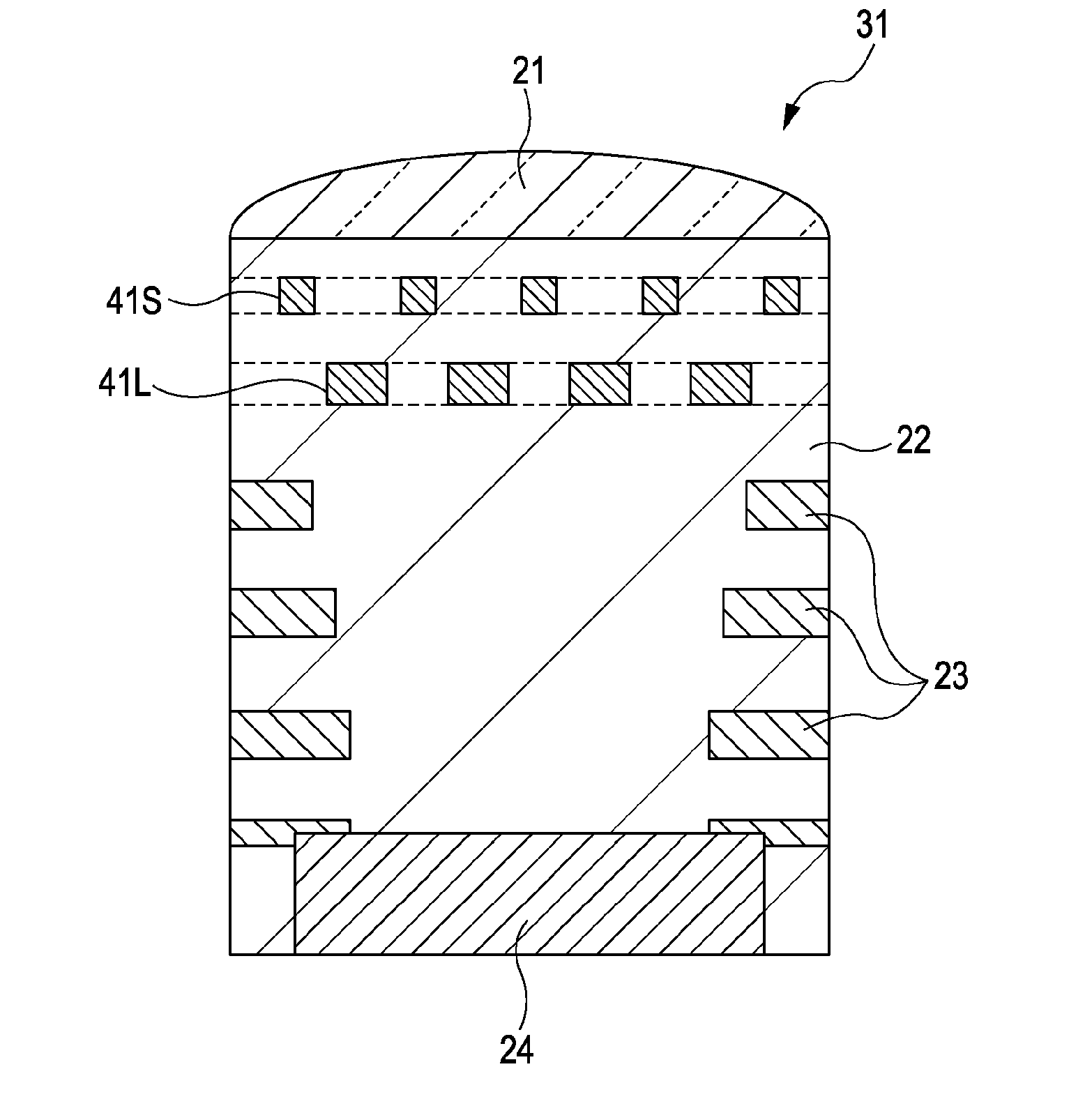
[0062]1. First embodiment (metal optical filters 41S and 41L are applied)

[0063]2. Second embodiment (a metal optical filter 41S and a thin film filter 61 are applied)

[0064]3. Third embodiment (a metal optical filter 41 is mounted in the same layer as metal wiring 23)

[0065]4. Fourth embodiment (a configuration different from those of the first to third embodiments is used as a configuration of a metal optical filter 41)

3. Solid-State Imaging Device According to First Embodiment of the Present Invention

[0066]FIG. 3 is a sectional view showing an example of a configuration of a pixel portion of a solid-state imaging device 31 according to a first embodiment of the present invention.

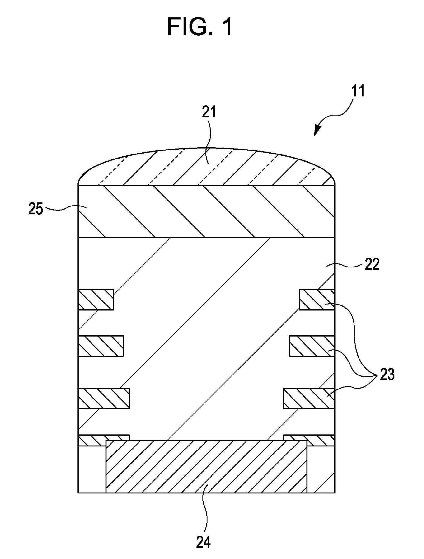
[0067]In FIG. 3, a portion corresponding to FIG. 1 is denoted by the same reference numeral. Description of such a portion is appropriately omitted. This applies to the drawings described below.

[0068]The pixel portion of the solid-state imaging device 31 is configured to include an on-chip light-collecting e...


PUM


Abstract

An optical element includes a first filter having the function to transmit a component at a lower frequency than a first cutoff frequency in incident light, a second filter having the function to transmit a component at a higher frequency than a second cutoff frequency in the incident light, and a light-receiving element for photoelectrically converting the components transmitted through the first filter and the second filter in the incident light. A metal optical filter composed of a conductor thin film is used as at least one of the first filter and the second filter.

Description

BACKGROUND OF THE INVENTION[0001]1. Field of the Invention[0002]The present invention relates to an optical element and a solid-state imaging device and particularly to an optical element and a solid-state imaging device which permit a technique of selectively extracting only an electromagnetic component at a specified wavelength to be realized by a chemically stable, low-cost, lower-profile structure.[0003]2. Description of the Related Art[0004]Electronic devices including solid-state imaging devices for imaging by photographing objects, such as a digital still camera, a camcorder, and the like, have recently increased. Currently mainstream solid-state imaging devices include a CCD (Charge Coupled Device) image sensor, a CMOS (Complementary Metal Oxide Semiconductor) image sensor, and the like. Hereinafter, these solid-state imaging devices are collectively named “CCD / CMOS image sensors”. The CCD / CMOS image sensors have sensitivity in a wide range from a visible wavelength to a nea...

Claims


Application Information

Patent Timeline
Patent Type & Authority Patents(United States)
IPC IPC(8): H01L27/00
CPCG02B5/201G02B5/204H01L27/14627H01L27/14621H01L27/14636
Inventor YOKOGAWA, SOZO
Owner SONY SEMICON SOLUTIONS CORP
Learn More