Two-dimensional solid-state image capture device and polarization-light data processing method therefor

Active Publication Date: 2010-11-11
SONY SEMICON SOLUTIONS CORP
View PDF7 Cites 96 Cited by
  • Summary
  • Abstract
  • Description
  • Claims
  • Application Information

AI Technical Summary

Benefits of technology

[0024]In the two-dimensional solid-state image capture device according to the first mode of the present invention, the polarization member and the wiring member for controlling the operation of the photoelectric conversion element are made of the same material and are disposed on the same virtual plane. Thus, the wiring layer and the polarization member can be simultaneously formed in the same process. That is, the positional relationship between the wire-grid polarization member and the wiring layer in the manufacturing process is optimized, thus making it possible to provide the polarization member without an increase in the number of manufacturing processes and making it possible to reduce the manufacturing cost of the two-dimensional solid-state image capture device. In the two-dimensional solid-state image capture device according to the second mode of the present invention, the polarization member and the light-shielding layer for controlling (restricting) incidence of light on the photoelectric conversion element are disposed on the same virtual plane. Thus, the light-shielding layer and the polarization member can be simultaneously formed in the same process. That is, the positional relationship between the wire-grid polarization member and the light-shielding layer in the manufacturing process is optimized, thus making it possible to reduce the manufacturing cost of the two-dimensional solid-state image capture device. Thus, the two-dimensional solid-state image capture device according to the first or second mode of the present invention can be manufactured using a general semiconductor-device manufacturing process. Moreover, since it is not necessary to add another layer for the polarization member, it is possible to achieve a lower-profile structure of the two-dimensional solid-state image capture device. The provision of the polarization member also does not involve an increase in the thickness of the two-dimensional solid-state image capture device. In addition, in the two-dimensional solid-state image capture device in the third mode of the present invention, the color filter and the polarization member are disposed on the same virtual plane. Thus, it is unlikely that the height of th

Problems solved by technology

As the thickness of the polarization element increases, oblique-incident-light-induced color mixture with neighborhood pixels and a sensitivity decrease due to attenuation/diffusion of light propagating in a medium become more problematic.
Hence, the technology lacks feasibility.
On the other hand, Japanese Unexamined Patent Application Publication (Translation of PCT Application) No. 2007-501391 employs a wire grid (a conductor lattice) as an optical element for a near-field ligh

Method used


Image

  • Two-dimensional solid-state image capture device and polarization-light data processing method therefor
  • Two-dimensional solid-state image capture device and polarization-light data processing method therefor
  • Two-dimensional solid-state image capture device and polarization-light data processing method therefor

Examples


first embodiment

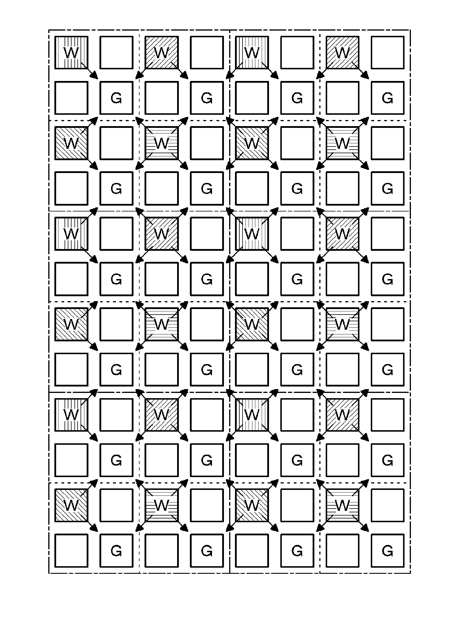
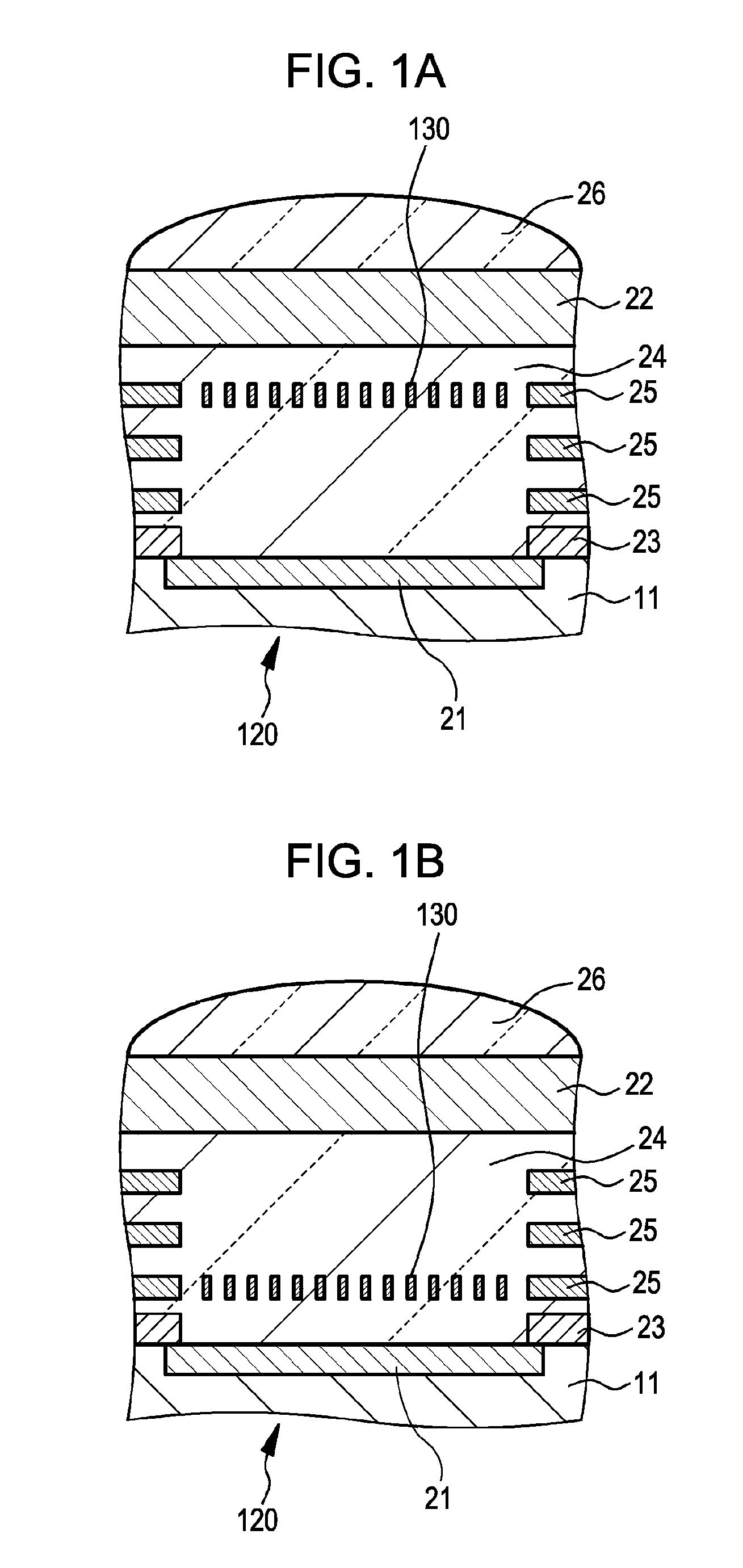
[0061]A first embodiment relates to a two-dimensional solid-state image capture device according to a first mode and a fourth mode of the present invention and to a polarization-light data processing method for the two-dimensional solid-state image capture device according to the first mode of the present invention. FIGS. 1A and 1B show partial schematic cross-sectional views of the two-dimensional solid-state image capture device in the first embodiment, FIGS. 5 to 9 schematically show plan layout views of sub-pixel regions 120 in the first embodiment, and FIGS. 4A and 4B are partial plan views of a polarization member 130.

[0062]In a two-dimensional solid-state image capture device in the first embodiment or each of the second to fourth embodiments described below, multiple pixel areas are generally arranged in a two-dimensional matrix in an X direction and a Y direction and each pixel area is constituted by multiple (M0) sub-pixel regions 120, where M0=4 in the embodiment. Each su...

second embodiment

[0092]A second embodiment relates to a polarization-light data processing method for a two-dimensional solid-state image capture device according to a second mode of the present invention. The two-dimensional solid-state image capture device in the second embodiment may have the same configuration as the two-dimensional solid-state image capture device described above in the first embodiment, and thus, a detailed description is not given hereinafter.

[0093]The polarization-light data processing method for the two-dimensional solid-state image capture device in the second embodiment is a simplified one of the polarization-light data processing method for the two-dimensional solid-state image capture device in the first embodiment, thereby achieving a reduction in the amount of data processing. In the polarization-light data processing method for the two-dimensional solid-state image capture device in the second embodiment, Iq denotes the light intensity of light that is incident on th...

third embodiment

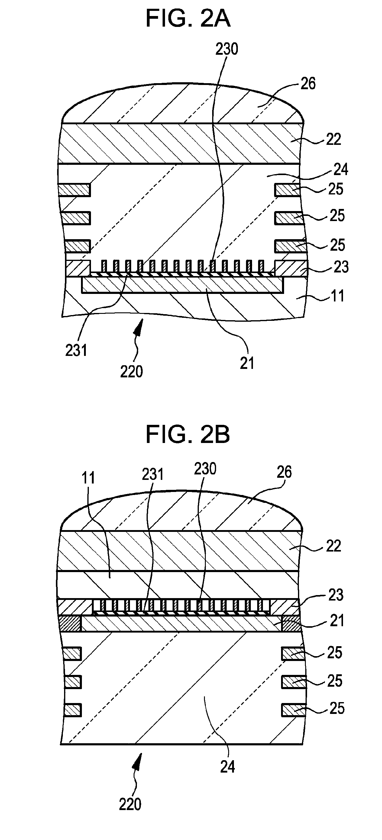
[0095]A third embodiment relates to the two-dimensional solid-state image capture device according to the second mode of the present invention. In the two-dimensional solid-state image capture device in the third embodiment, as shown in a schematic partial cross sectional view in FIG. 2A or 2B, a polarization member 230 is disposed at the light inside side of at least one of sub-pixel regions 220 constituting each pixel area. Each sub-pixel region has a light-shielding layer 23 for controlling (restricting) incidence of light on the photoelectric conversion element. The polarization member 230 and the light-shielding layer 23 are disposed on the same virtual plane. In this case, the polarization member 230 is a wire-grid polarization member and is made of, for example, aluminum (Al) or copper (Cu), and the light-shielding layer 23 is made of, for example, aluminum (Al) or tungsten (W).

[0096]The two-dimensional solid-state image capture device shown in FIG. 2A is a frontside-illumina...


PUM


Abstract

A two-dimensional solid-state image capture device includes pixel areas arranged in a two-dimensional matrix, each pixel area being constituted by multiple sub-pixel regions, each sub-pixel region having a photoelectric conversion element. A polarization member is disposed at a light incident side of at least one of the sub-pixel regions constituting each pixel area. The polarization member has strip-shaped conductive light-shielding material layers and slit areas, provided between the strip-shaped conductive light-shielding material layers. Each sub-pixel region further has a wiring layer for controlling an operation of the photoelectric conversion element, and the polarization member and the wiring layer are made of the same material and are disposed on the same virtual plane.

Description

BACKGROUND OF THE INVENTION[0001]1. Field of the Invention[0002]The present invention relates to a two-dimensional solid-state image capture device and a polarization-light data processing method therefor.[0003]2. Description of the Related Art[0004]Two-dimensional solid-state image capture devices that obtain images through photography of subjects by using photoelectric conversion elements including two-dimensional solid-state image capture elements are increasingly used. Examples include a digital still camera, a video camera, and a camcorder (which is an integration of a photographing unit (such as a video camera) and a recording unit, and which is an abbreviation of a camera and recorder). CCD (charge coupled device) image capture elements and CMOS (complementary metal oxide semiconductor) image capture elements, which are solid-state image capture elements mainly used today, have sensitivities in a wide range from a visible-light wavelength to a near-infrared-light wavelength a...

Claims


Application Information

Patent Timeline
IPC IPC(8): G01J4/00H01L27/14H01L27/146H01L27/148H04N5/335H04N5/369H04N5/372H04N5/374
CPCH01L27/14621H01L27/14625H01L27/14685H04N5/335H04N2209/046H04N5/235H04N9/045H01L27/14623H04N25/133H04N25/135H04N25/00
Inventor YOKOGAWA, SOZO
Owner SONY SEMICON SOLUTIONS CORP
Why Eureka
Try Eureka