

Optical element and solid-state imaging device
a solid-state imaging and optical element technology, applied in the direction of optical radiation measurement, instruments, spectrometry/spectrophotometry/monochromators, etc., can solve the problems of carbon-hydrogen bond breakage and carbon-bond breakage, and achieve the effect of a lower-profile structur
- Summary
- Abstract
- Description
- Claims
- Application Information
AI Technical Summary
Benefits of technology
Problems solved by technology
Method used
Image

Examples
first embodiment (
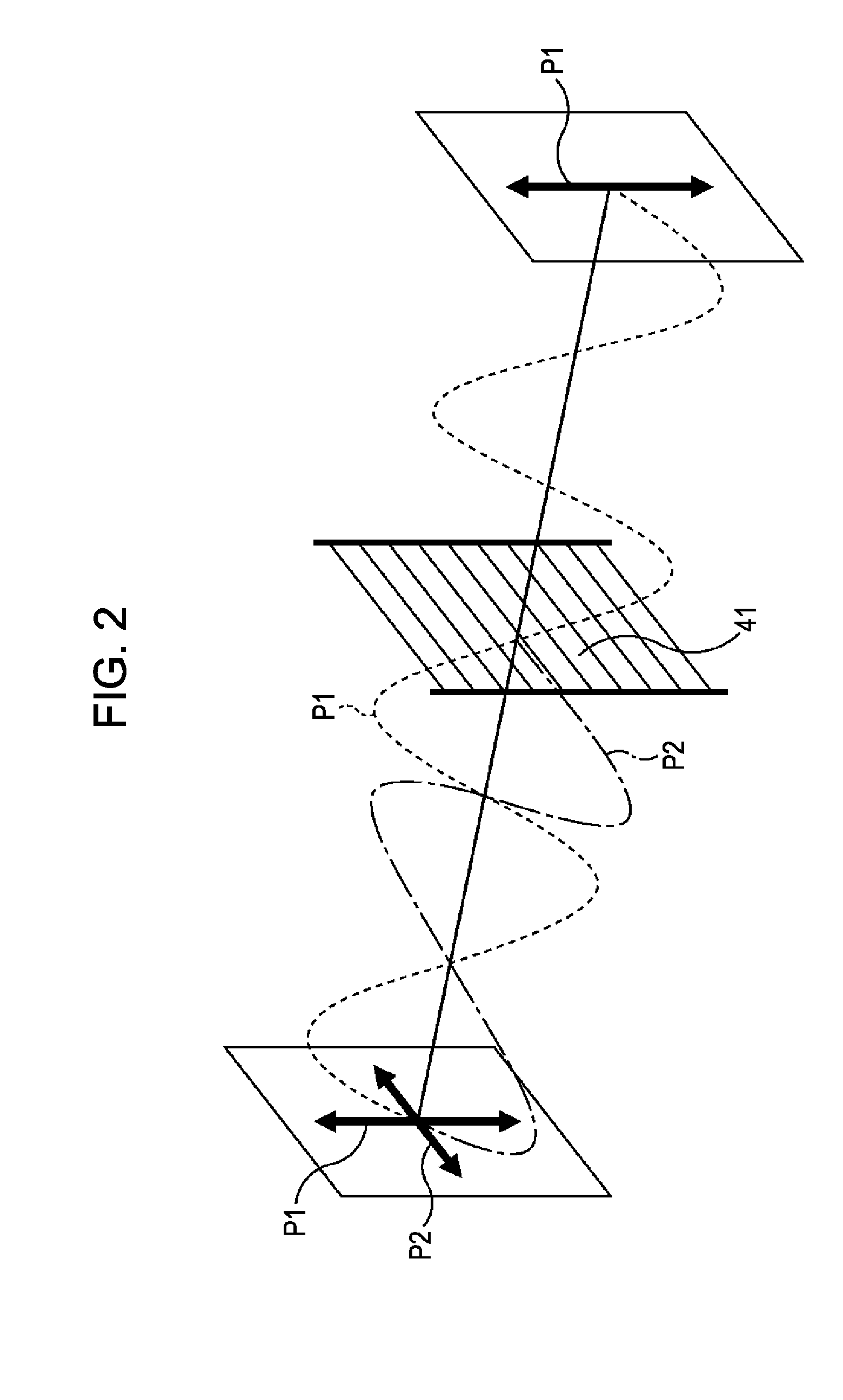
[0062]1. First embodiment (metal optical filters 41S and 41L are applied)
[0063]2. Second embodiment (a metal optical filter 41S and a thin film filter 61 are applied)
[0064]3. Third embodiment (a metal optical filter 41 is mounted in the same layer as metal wiring 23)
[0065]4. Fourth embodiment (a configuration different from those of the first to third embodiments is used as a configuration of a metal optical filter 41)
3. Solid-State Imaging Device According to First Embodiment of the Present Invention
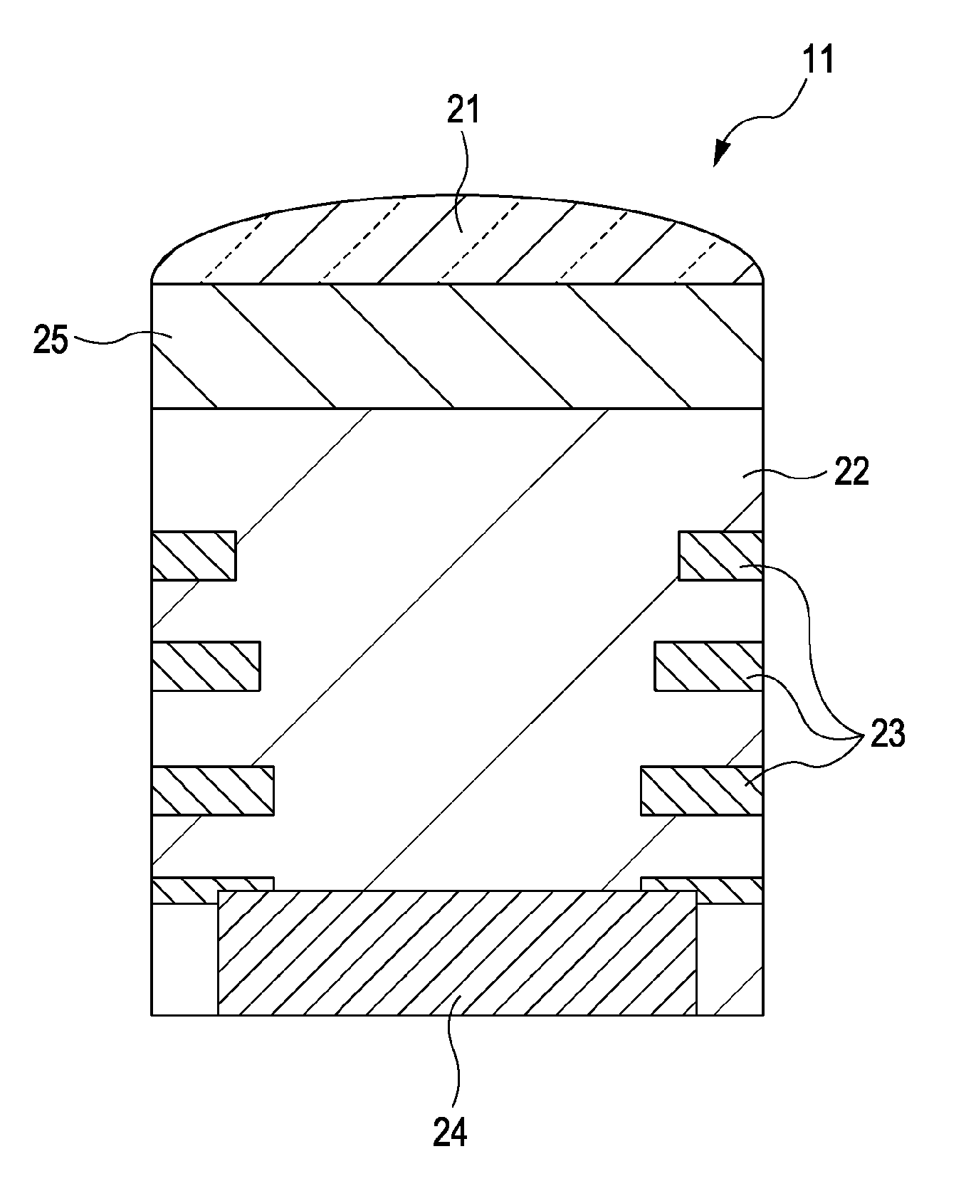
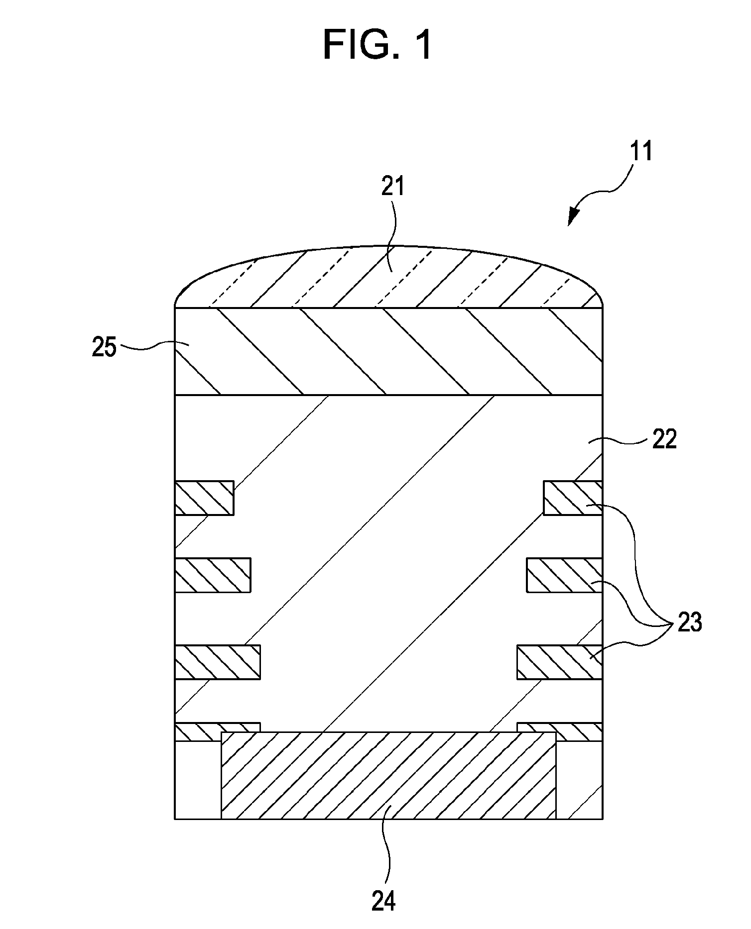
[0066]FIG. 3 is a sectional view showing an example of a configuration of a pixel portion of a solid-state imaging device 31 according to a first embodiment of the present invention.
[0067]In FIG. 3, a portion corresponding to FIG. 1 is denoted by the same reference numeral. Description of such a portion is appropriately omitted. This applies to the drawings described below.
[0068]The pixel portion of the solid-state imaging device 31 is configured to include an on-chip light-collecting e...
PUM
 Abstract
Description
Claims
Application Information