Two-dimensional solid-state image capture device with polarization member and color filter for sub-pixel regions

a two-dimensional solid-state image and sub-pixel technology, applied in the direction of radiation controlled devices, optical radiation measurement, instruments, etc., can solve the problems of attenuation, sensitivity decrease due to attenuation, and difficulty in achieving the effect of reducing the manufacturing cost of the two-dimensional solid-state image capture devi

Active Publication Date: 2014-06-24
SONY SEMICON SOLUTIONS CORP
View PDF8 Cites 15 Cited by
  • Summary
  • Abstract
  • Description
  • Claims
  • Application Information

AI Technical Summary

Benefits of technology

[0015]Accordingly, it is desirable to provide a two-dimensional solid-state image capture device having an optimized positional relationship between the wire-grid polarization member and the wiring layer for controlling the operation of the photoelectric conversion element, an optimized positional relationship between the polarization member and the light-shielding layer for controlling (restricting) incidence of light on the photoelectric conversion element, and an optimized positional relationship between the polarization member and the color filter. It is also desirable to provide a two-dimensional solid-state image capture device having a configuration and a structure with which a decrease in the sensitivity is unlikely. It is further desirable to provide a polarization-light data processing method that is applied for a two-dimensional solid-state image capture device having a configuration and a structure with which a decrease in the sensitivity is unlikely and that does not complicate computation processing for the amount and intensity of light received by the photoelectric conversion element.
[0016]A two-dimensional solid-state image capture device according to first to fourth modes of the present invention includes: pixel areas arranged in a two-dimensional matrix, each pixel area being constituted by multiple sub-pixel regions, each sub-pixel region having a photoelectric conversion element. The polarization member has strip-shaped conductive light-shielding material layers and slit areas, provided between the strip-shaped conductive light-shielding material layers, to transmit light having a polarization component in a direction perpendicular to a direction in which the strip-shaped conductive light-shielding material layers extend and to suppress transmission of light having a polarization component in a direction parallel to the direction in which the strip-shaped conductive light-shielding material layers extend.
[0024]In the two-dimensional solid-state image capture device according to the first mode of the present invention, the polarization member and the wiring member for controlling the operation of the photoelectric conversion element are made of the same material and are disposed on the same virtual plane. Thus, the wiring layer and the polarization member can be simultaneously formed in the same process. That is, the positional relationship between the wire-grid polarization member and the wiring layer in the manufacturing process is optimized, thus making it possible to provide the polarization member without an increase in the number of manufacturing processes and making it possible to reduce the manufacturing cost of the two-dimensional solid-state image capture device. In the two-dimensional solid-state image capture device according to the second mode of the present invention, the polarization member and the light-shielding layer for controlling (restricting) incidence of light on the photoelectric conversion element are disposed on the same virtual plane. Thus, the light-shielding layer and the polarization member can be simultaneously formed in the same process. That is, the positional relationship between the wire-grid polarization member and the light-shielding layer in the manufacturing process is optimized, thus making it possible to reduce the manufacturing cost of the two-dimensional solid-state image capture device. Thus, the two-dimensional solid-state image capture device according to the first or second mode of the present invention can be manufactured using a general semiconductor-device manufacturing process. Moreover, since it is not necessary to add another layer for the polarization member, it is possible to achieve a lower-profile structure of the two-dimensional solid-state image capture device. The provision of the polarization member also does not involve an increase in the thickness of the two-dimensional solid-state image capture device. In addition, in the two-dimensional solid-state image capture device in the third mode of the present invention, the color filter and the polarization member are disposed on the same virtual plane. Thus, it is unlikely that the height of the sub-pixel region having the polarization member and the height of another sub-pixel region having the color filters differ from each other. Since the thickness of the polarization member in the two-dimensional solid-state image capture device in each of the first to third modes of the present invention can be reduced to as small as about 0.1 μm, it is possible to more realizably achieve a lower-profile structure of the two-dimensional solid-state image capture device.
[0025]The polarization member transmits only polarization components in a particular direction and reflects and absorbs other polarization components. Thus, the sub-pixel region having the polarization member has a problem in that the sensitivity decreases compared to the sub-pixel region having no polarization member. In the two-dimensional solid-state image capture device according to the fourth mode of the present invention and the two-dimensional solid-state image capture device in the polarization-light data processing method according to the first or second mode of the present invention, the polarization member is disposed at the light incident side of one of the multiple (M0) sub-pixel regions constituting each pixel area and Q polarization members (where Q≦Q0) are disposed in the pixel-area group constituted by Q pixel areas (where Q0≧3). That is, only Q polarization members are disposed in the total of Q0×M0 sub-pixel regions constituting one pixel-area group. Consequently, it is possible to minimize a sensitivity reduction due to the arrangement of the polarization members in the entire pixel area. Determination of the polarization direction and the intensity of polarization components (the polarization component intensity) at the position of each pixel area by performing inter-pixel-area computation processing makes it possible to obtain polarization information with the spatial resolution being slightly compromised, while minimizing a reduction in the sensitivity. Since only Q polarization members are disposed in the total of Q0×M0 sub-pixel regions constituting one pixel-area group, the computation processing for the amount and intensity of light received by the photoelectric conversion elements does not become complicated.

Problems solved by technology

As the thickness of the polarization element increases, oblique-incident-light-induced color mixture with neighborhood pixels and a sensitivity decrease due to attenuation / diffusion of light propagating in a medium become more problematic.
Hence, the technology lacks feasibility.
On the other hand, Japanese Unexamined Patent Application Publication (Translation of PCT Application) No. 2007-501391 employs a wire grid (a conductor lattice) as an optical element for a near-field light detection sensor, but is not aimed to obtain polarization information and also does not explain a method for disposing three or more types of polarization element used for obtaining polarization information and an algorithm used for extracting the polarization information.
This arrangement has some problems.
Additionally, the computation processing for the amount and intensity of light received by the photoelectric conversion element in each sub-pixel region becomes complicated.

Method used


Image

  • Two-dimensional solid-state image capture device with polarization member and color filter for sub-pixel regions
  • Two-dimensional solid-state image capture device with polarization member and color filter for sub-pixel regions
  • Two-dimensional solid-state image capture device with polarization member and color filter for sub-pixel regions

Examples


first embodiment

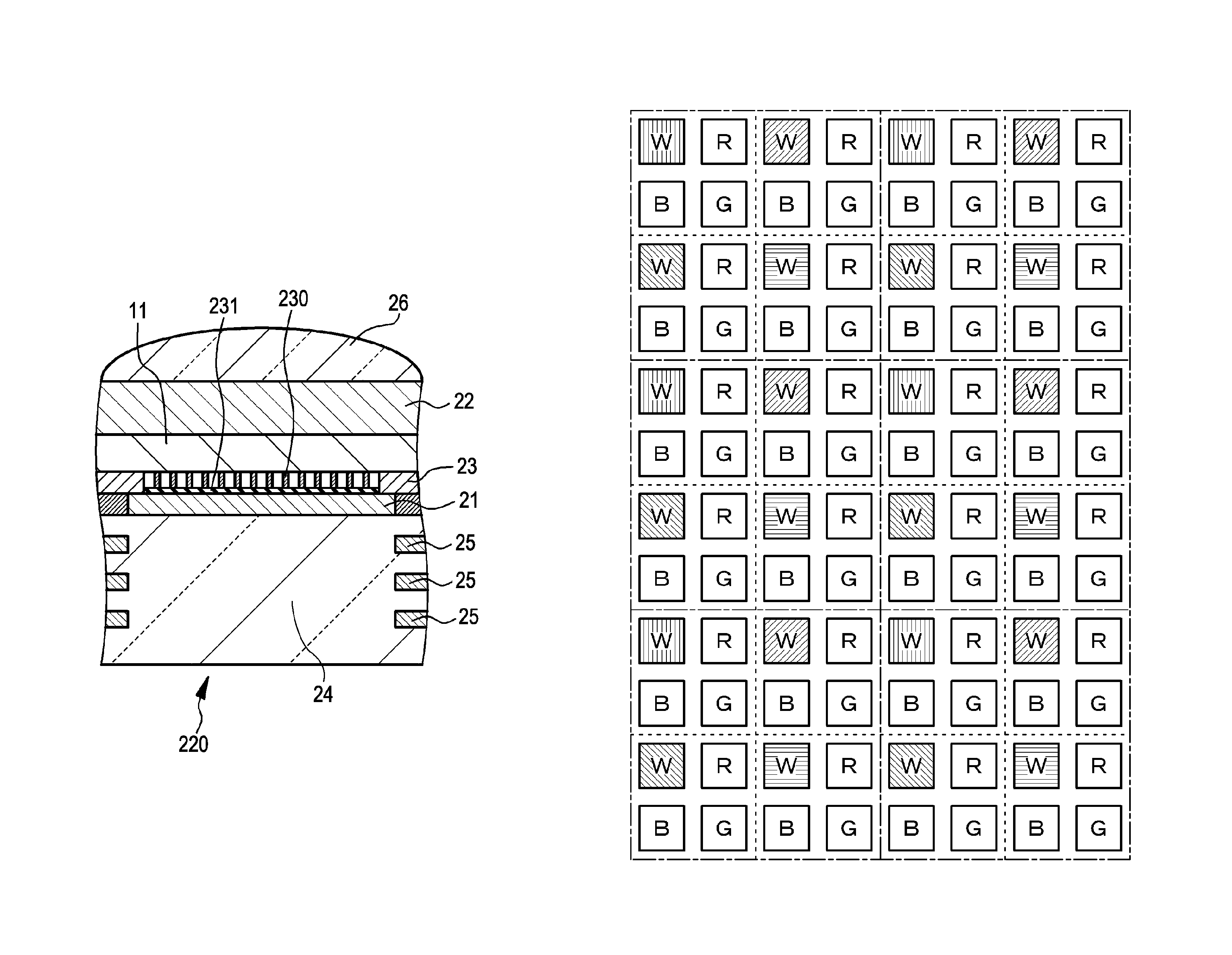
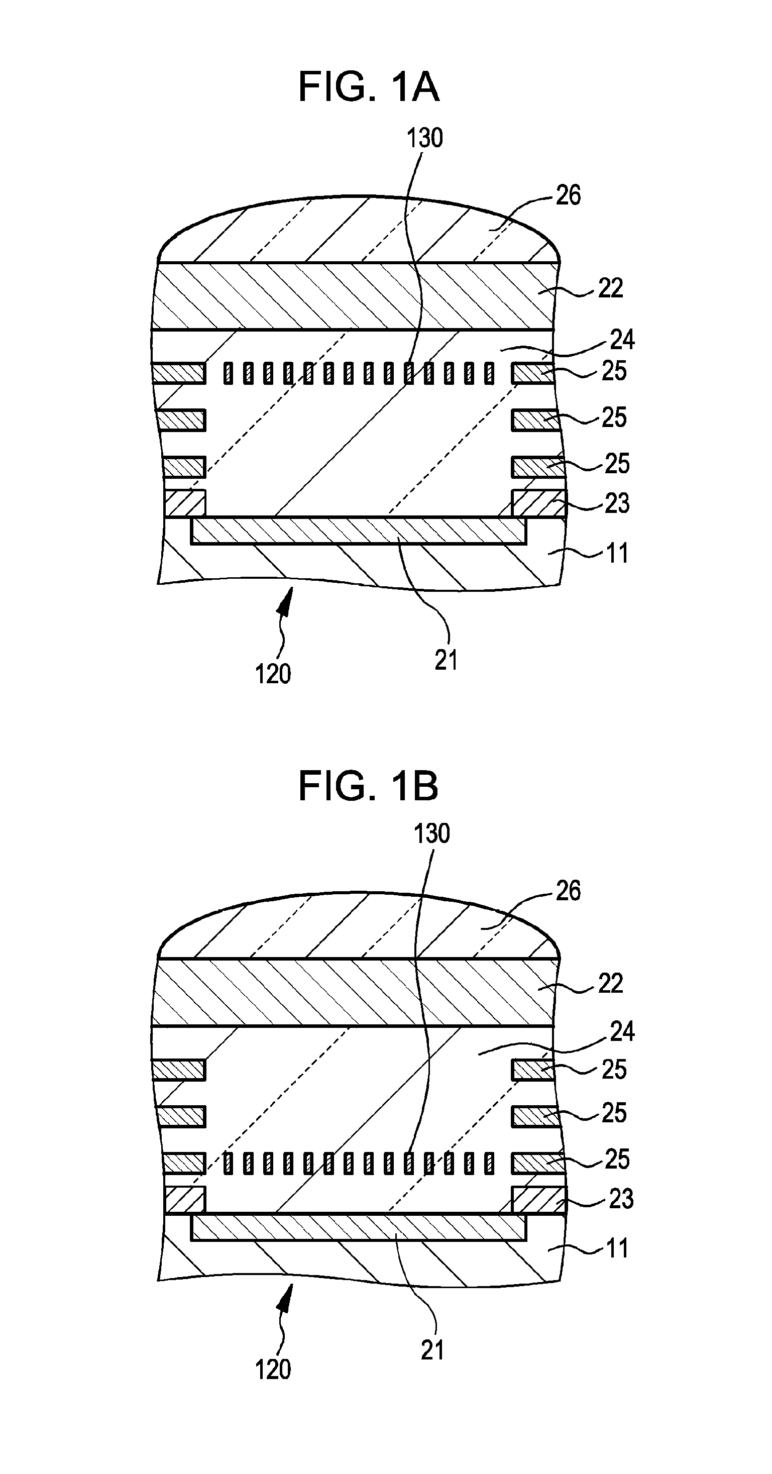
[0062]A first embodiment relates to a two-dimensional solid-state image capture device according to a first mode and a fourth mode of the present invention and to a polarization-light data processing method for the two-dimensional solid-state image capture device according to the first mode of the present invention. FIGS. 1A and 1B show partial schematic cross-sectional views of the two-dimensional solid-state image capture device in the first embodiment, FIGS. 5 to 9 schematically show plan layout views of sub-pixel regions 120 in the first embodiment, and FIGS. 4A and 4B are partial plan views of a polarization member 130.

[0063]In a two-dimensional solid-state image capture device in the first embodiment or each of the second to fourth embodiments described below, multiple pixel areas are generally arranged in a two-dimensional matrix in an X direction and a Y direction and each pixel area is constituted by multiple (M0) sub-pixel regions 120, where M0=4 in the embodiment. Each su...

second embodiment

[0093]A second embodiment relates to a polarization-light data processing method for a two-dimensional solid-state image capture device according to a second mode of the present invention. The two-dimensional solid-state image capture device in the second embodiment may have the same configuration as the two-dimensional solid-state image capture device described above in the first embodiment, and thus, a detailed description is not given hereinafter.

[0094]The polarization-light data processing method for the two-dimensional solid-state image capture device in the second embodiment is a simplified one of the polarization-light data processing method for the two-dimensional solid-state image capture device in the first embodiment, thereby achieving a reduction in the amount of data processing. In the polarization-light data processing method for the two-dimensional solid-state image capture device in the second embodiment, Iq denotes the light intensity of light that is incident on th...

third embodiment

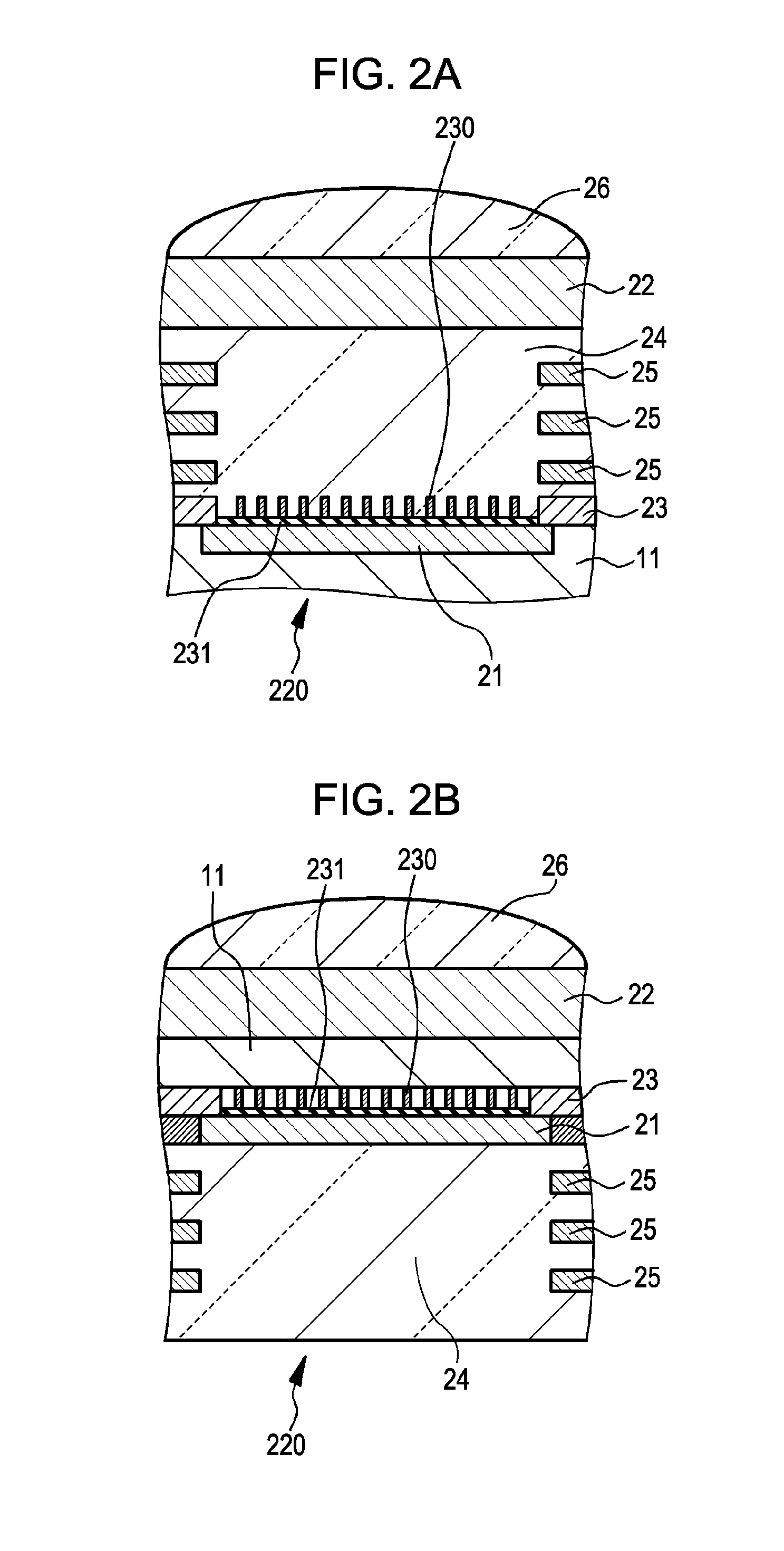
[0096]A third embodiment relates to the two-dimensional solid-state image capture device according to the second mode of the present invention. In the two-dimensional solid-state image capture device in the third embodiment, as shown in a schematic partial cross sectional view in FIG. 2A or 2B, a polarization member 230 is disposed at the light inside side of at least one of sub-pixel regions 220 constituting each pixel area. Each sub-pixel region has a light-shielding layer 23 for controlling (restricting) incidence of light on the photoelectric conversion element. The polarization member 230 and the light-shielding layer 23 are disposed on the same virtual plane. In this case, the polarization member 230 is a wire-grid polarization member and is made of, for example, aluminum (Al) or copper (Cu), and the light-shielding layer 23 is made of, for example, aluminum (Al) or tungsten (W).

[0097]The two-dimensional solid-state image capture device shown in FIG. 2A is a frontside-illumina...


PUM

PropertyMeasurementUnit
wavelengthsaaaaaaaaaa
width WCaaaaaaaaaa
wavelengths λRaaaaaaaaaa

Abstract

A two-dimensional solid-state image capture device includes pixel areas arranged in a two-dimensional matrix, each pixel area being constituted by multiple sub-pixel regions, each sub-pixel region having a photoelectric conversion element. A polarization member is disposed at a light incident side of at least one of the sub-pixel regions constituting each pixel area. The polarization member has strip-shaped conductive light-shielding material layers and slit areas, provided between the strip-shaped conductive light-shielding material layers. Each sub-pixel region further has a wiring layer for controlling an operation of the photoelectric conversion element, and the polarization member and the wiring layer are made of the same material and are disposed on the same virtual plane.

Description

BACKGROUND OF THE INVENTION[0001]1. Field of the Invention[0002]The present invention relates to a two-dimensional solid-state image capture device and a polarization-light data processing method therefor.[0003]2. Description of the Related Art[0004]Two-dimensional solid-state image capture devices that obtain images through photography of subjects by using photoelectric conversion elements including two-dimensional solid-state image capture elements are increasingly used. Examples include a digital still camera, a video camera, and a camcorder (which is an integration of a photographing unit (such as a video camera) and a recording unit, and which is an abbreviation of a camera and recorder). CCD (charge coupled device) image capture elements and CMOS (complementary metal oxide semiconductor) image capture elements, which are solid-state image capture elements mainly used today, have sensitivities in a wide range from a visible-light wavelength to a near-infrared-light wavelength a...

Claims


Application Information

Patent Timeline
Patent Type & Authority Patents(United States)
IPC IPC(8): H01L27/14H01L27/148H04N5/369G02F1/01H04N5/372H04N5/335H01L27/00H04N5/374H01L27/146G01J3/51
CPCH04N9/045H01L27/14621H04N2209/046H04N5/235H01L27/14685H01L27/14625H04N5/335H01L27/14623H04N25/133H04N25/135H04N25/00
Inventor YOKOGAWA, SOZO
Owner SONY SEMICON SOLUTIONS CORP
Why Eureka
Try Eureka