Wiring nanoscale sensors with nanomechanical resonators

a nanomechanical resonator and nanoscale sensor technology, applied in the field of semiconductors, to achieve the effect of solving the wiring problem

Active Publication Date: 2013-01-08
CALIFORNIA INST OF TECH
View PDF13 Cites 14 Cited by
  • Summary
  • Abstract
  • Description
  • Claims
  • Application Information

AI Technical Summary

Problems solved by technology

A multitude of promising nanoscale electronic devices have been developed for the implementation of gain1, digital logic2 and analog sensing.3-5 Yet far less attention has been directed on how to interface systems built from these components with the macroscopic world.6-9 The top-down wiring problem raises several challenges related to the integration of very large systems with a miniscule footprint.

Method used


Image

  • Wiring nanoscale sensors with nanomechanical resonators
  • Wiring nanoscale sensors with nanomechanical resonators
  • Wiring nanoscale sensors with nanomechanical resonators

Examples


Embodiment Construction

[0039]In the following description, reference is made to the accompanying drawings which form a part hereof, and which is shown, by way of illustration, several embodiments of the present invention. It is understood that other embodiments may be utilized and structural changes may be made without departing from the scope of the present invention.

Overview

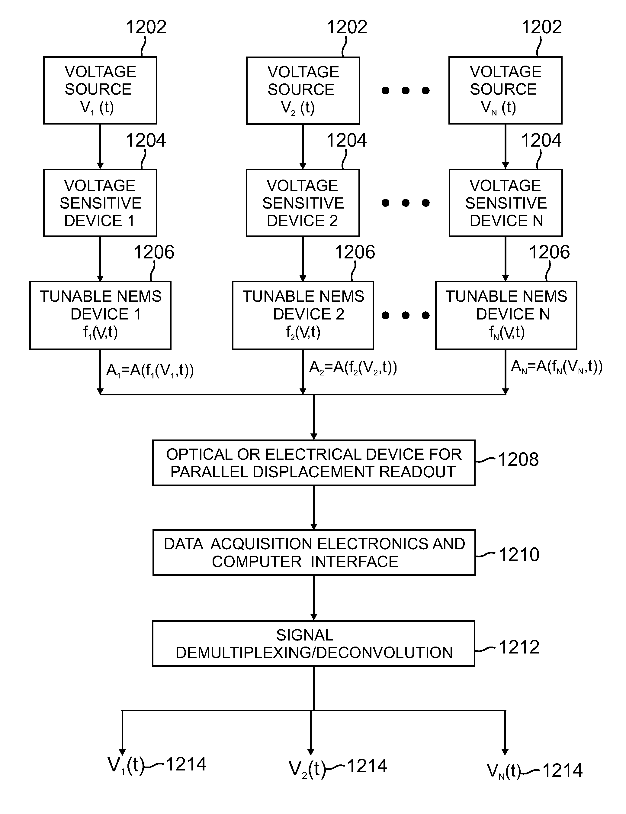
[0040]Embodiments of the present invention provide a new paradigm for wiring nanoscale sensor arrays to the macroscopic world, employing frequency-sensitive nanoelectromechanical systems (NEMS) coupled to a single output line (output line is also known as an output path or signal transmission line). Potentially, thousands of sensor channels could be multiplexed in parallel, thereby greatly alleviating the wiring constraints that arise with scaling up device complexity.

[0041]Detailed Description

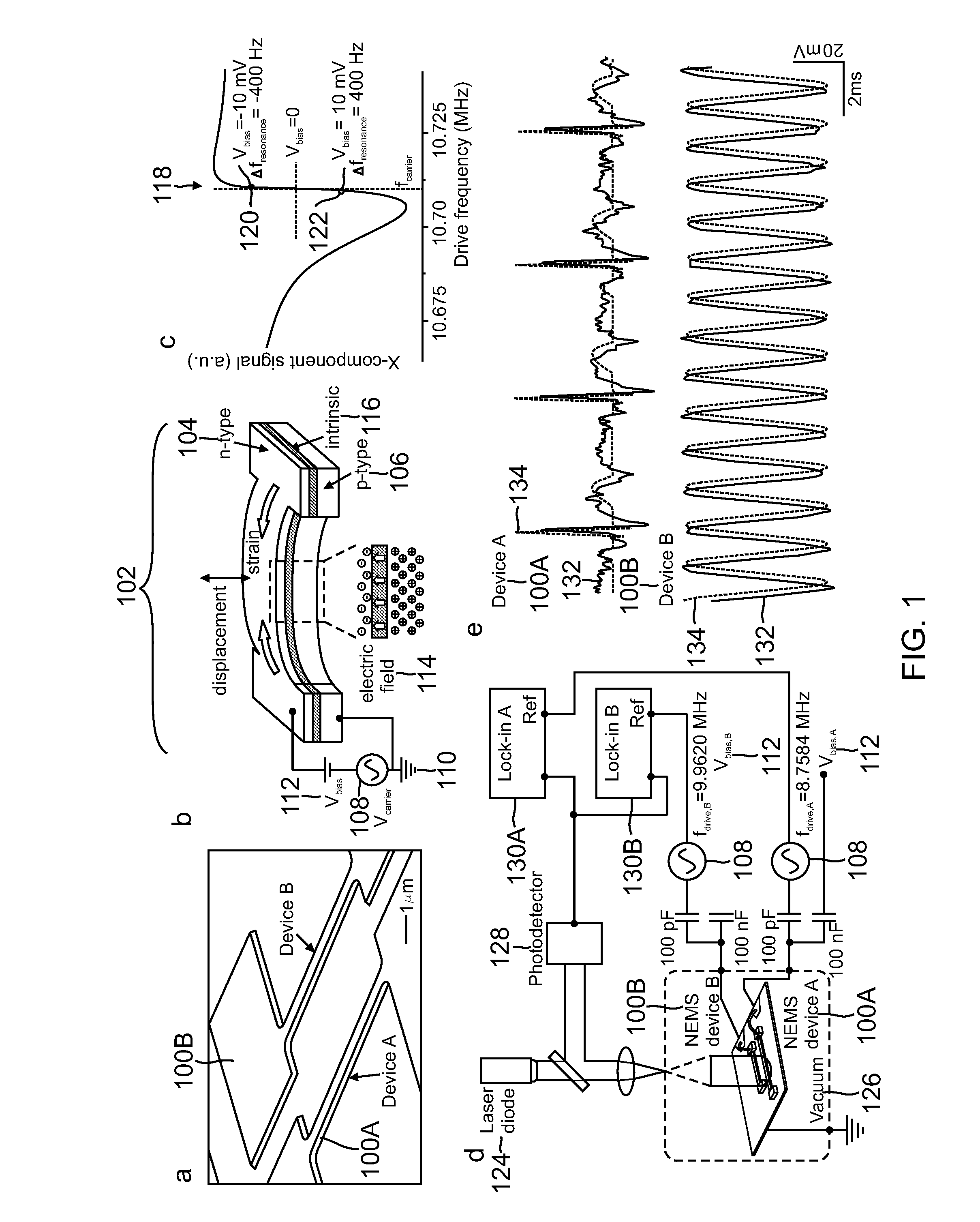
[0042]One or more embodiments of the invention may be viewed as conceptually similar to the mechanism of action of the cochlea in the inner ea...


PUM


Abstract

A system, device, method, and apparatus provide the ability to wire a voltage sensitive device to a nanoelectromechanical system (NEMS) resonator. A voltage sensitive device is configured to detect one or more voltage signals and output one or more electrical potentials in real-time. An array of piezoelectric NEMS resonators (with each resonator tuned to a unique frequency) is used to receive the output electrical potentials and convert each output electrical potential to a corresponding resonance frequency varying signal. The output signal from each resonator varies in linear proportion to the resonator's corresponding frequency variation arising from the applied electrical potential. The frequency varying signals are multiplexed together into a single readout signal path that is monitored to determine variations in vibrational amplitude. A demodulation device deconvolves the multiplexed frequency varying signals to recover and uniquely identify the output electrical signal.

Description

CROSS-REFERENCE TO RELATED APPLICATIONS[0001]This application claims the benefit under 35 U.S.C. Section 119(e) of the following commonly-assigned U.S. provisional patent application(s), which is / are incorporated by reference herein:[0002]Provisional Application Ser. No. 61 / 208,805, filed on Feb. 27, 2009, by Akram S. Sadek, Rassul Karabalin, Michael L. Roukes, and Sotirios K. Masmanidis, entitled “Piezoelectric, Voltage-Sensitive Nanomechanical Systems for Frequency-Modulated, Multiplexed Electrical Signal Transmission in Extracellular Electrode Arrays for Neural Recording Applications”.[0003]This application is related to the following commonly-assigned patent applications, which applications are incorporated by reference herein:[0004]U.S. patent application Ser. No. 11 / 830,653, entitled “HIGHLY EFFICIENT, CHARGE DEPLETION-MEDIATED, VOLTAGE-TUNABLE ACTUATION EFFICIENCY AND RESONANCE FREQUENCY OF PIEZOELECTRIC SEMICONDUCTOR NANOELECTROMECHANICAL SYSTEMS RESONATORS”, by Sotirios K. ...

Claims


Application Information

Patent Timeline
Patent Type & Authority Patents(United States)
IPC IPC(8): G01R29/22H01L41/00G01R23/00
CPCA61B5/04001H03H9/02259A61B5/0031A61B5/0492A61B2562/028A61B2562/0285H03H2009/241A61B5/24A61B5/296
Inventor SADEK, AKRAM SARWATKARABALIN, RASSUL BULATOVICHROUKES, MICHAEL L.MASMANIDIS, SOTIRIOS K.
Owner CALIFORNIA INST OF TECH
Why Eureka
Try Eureka