Check patentability & draft patents in minutes with Patsnap Eureka AI!

Clock receiver in semiconductor integrated circuit and method of controlling the same

a clock receiver and integrated circuit technology, applied in the direction of generating/distributing signals, pulse techniques, instruments, etc., can solve the problems of power loss, large current consumption, and decrease in power efficiency of semiconductor integrated circuits

Active Publication Date: 2013-01-08
SK HYNIX INC
View PDF18 Cites 0 Cited by
  • Summary
  • Abstract
  • Description
  • Claims
  • Application Information

AI Technical Summary

Benefits of technology

The solution improves power efficiency by reducing current consumption in high frequency clock buffers during low frequency operations and enhances adaptability to different operation environments by selectively activating the appropriate clock buffer, thereby minimizing power loss.

Problems solved by technology

However, there are times when the semiconductor integrated circuit configured for the high frequency operation environment is not always placed in the high frequency operation environment wherein the semiconductor integrated circuit is placed in either a low frequency operation environment as well as the high frequency operation environment.
As a result, when the semiconductor integrated circuit configured for the high frequency operation environment is placed in the low frequency operation environment and having the clock receiver configured suitable for the high frequency operation environment, this configuration causes a large amount of current consumption, thereby decreasing power efficiency of the semiconductor integrated circuit.
Therefore, the conventional clock receiver in the semiconductor integrated circuit lacks adaptability to the operation environment, thereby causing loss of power.

Method used


Image

  • Clock receiver in semiconductor integrated circuit and method of controlling the same
  • Clock receiver in semiconductor integrated circuit and method of controlling the same
  • Clock receiver in semiconductor integrated circuit and method of controlling the same

Examples


Embodiment Construction

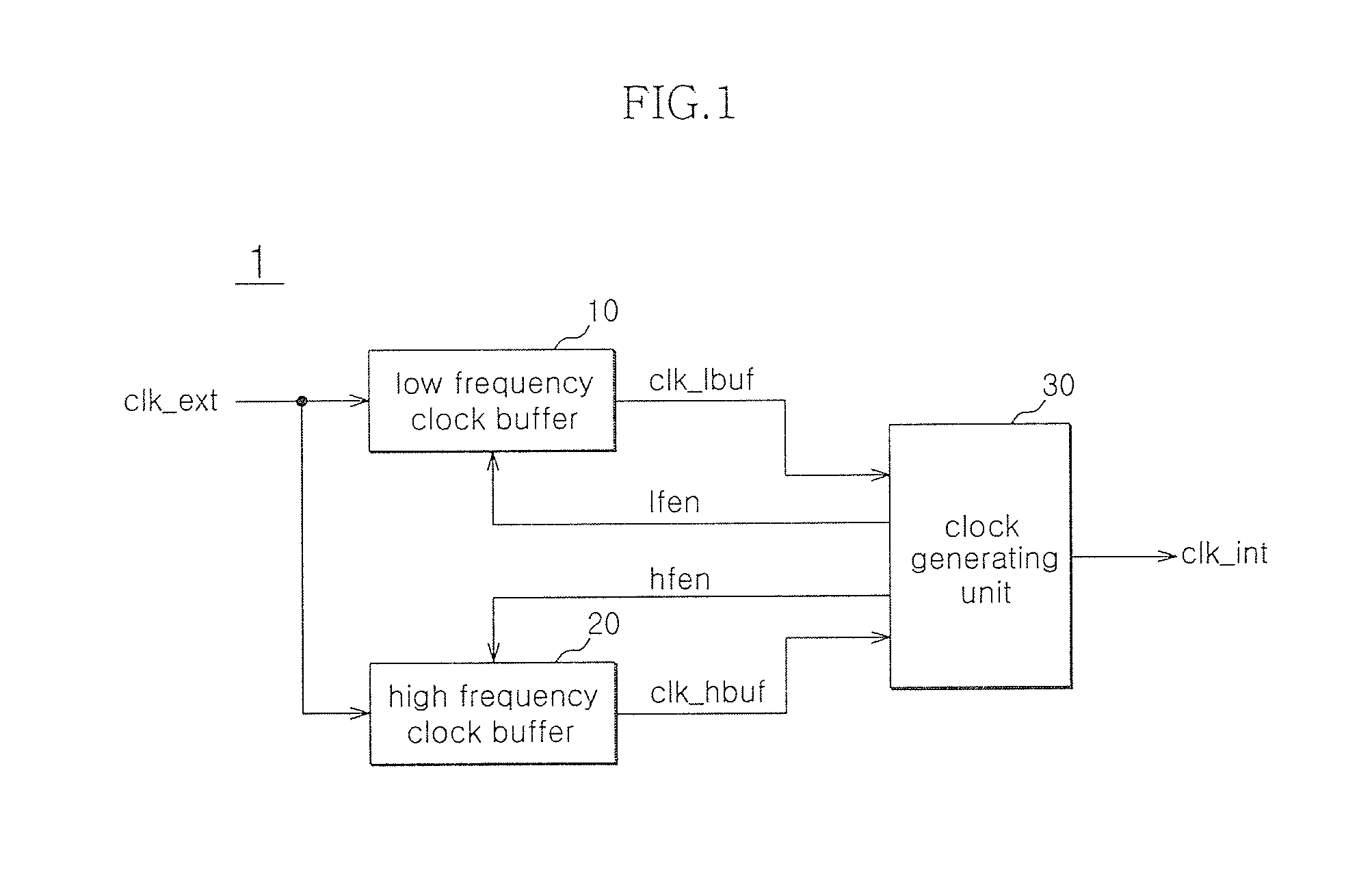
[0015]FIG. 1 is a block diagram showing a clock receiver 1 in a semiconductor integrated circuit according to an embodiment of the present invention.

[0016]As shown in FIG. 1, the clock receiver 1 includes a low frequency clock buffer 10, a high frequency clock buffer 20, and a clock generating unit 30.

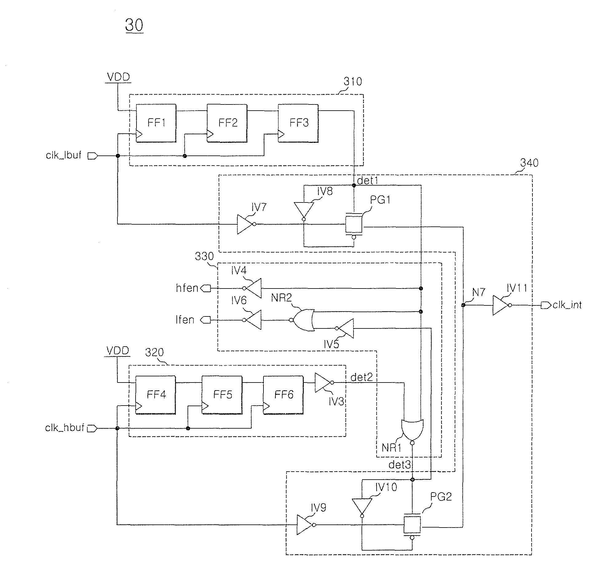
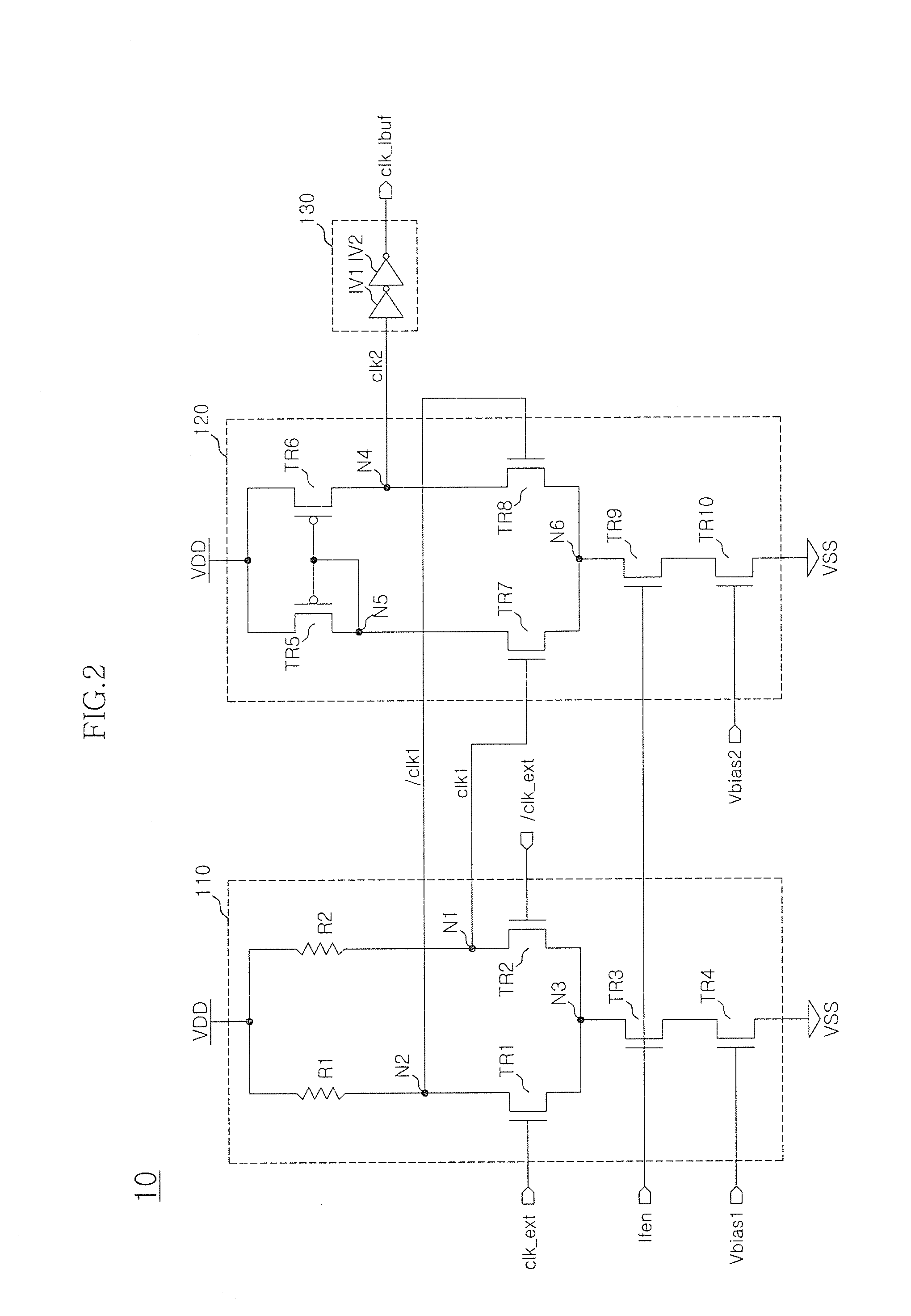
[0017]The low frequency clock buffer 10 performs a buffering operation in response to a low frequency operation signal ‘lfen’ to generate a low frequency buffered clock ‘clk_lbuf’. The high frequency clock buffer 20 performs a buffering operation in response to a high frequency operation signal ‘hfen’ to generate a high frequency buffered clock ‘clk_hbuf’. Then, the clock generating unit 30 receives the low frequency buffered clock ‘clk_lbuf’ and the high frequency buffered clock ‘clk_hbuf’, and controls states of the low frequency operation signal ‘lfen’ and the high frequency operation signal ‘hfen’ to generate an internal clock ‘clk_int’.

[0018]The clock generating unit 30 enables bo...


PUM


Abstract

A clock receiver in a semiconductor integrated circuit includes a first clock buffer configured to buffer an external clock to generate a low frequency buffered clock in response to a first operation signal; a second clock buffer configured to buffer the external clock to generate a high frequency buffered clock in response to a second operation signal; and an internal clock generating unit configured to receive the low frequency buffered clock and the high frequency buffered clock, to control states of the first operation signal and the second operation signal and to generate an internal clock.

Description

CROSS-REFERENCES TO RELATED APPLICATION[0001]The present application claims priority under 35 U.S.C. 119(a) to Korean application number 10-2009-0050796, filed on Jun. 9, 2009, in the Korean Patent Office, which is incorporated by reference in its entirety as if set forth in full.BACKGROUND[0002]1. Technical Field[0003]The embodiments described herein generally relate to a semiconductor integrated circuit, and more particularly, to a clock receiver in the semiconductor integrated circuit and a method of controlling the same.[0004]2. Related Art[0005]Typically, a semiconductor integrated circuit such as a Synchronous Dynamic Random Access Memory (SDRAM) has improved its operation speed by using a clock. For this improved operational speed, the semiconductor integrated circuit includes a clock buffer and buffers the clock inputted through a pad. In addition, the semiconductor integrated circuit uses the clock that is internally generated by compensating a phase difference with respect...

Claims


Application Information

Patent Timeline
Patent Type & Authority Patents(United States)
IPC IPC(8): H03L7/00
CPCG06F1/12G11C5/14G11C7/22G11C11/4074G11C11/4076
Inventor YUN, WON JOOLEE, HYUN WOOKIM, KI-HAN
Owner SK HYNIX INC
Features
  • R&D
  • Intellectual Property
  • Life Sciences
  • Materials
  • Tech Scout
  • Unparalleled Data Quality
  • Higher Quality Content
  • 60% Fewer Hallucinations
Learn More