Direct digital synthesis with reduced jitter

Active Publication Date: 2013-01-08
XILINX INC
View PDF11 Cites 5 Cited by
  • Summary
  • Abstract
  • Description
  • Claims
  • Application Information

AI Technical Summary

Benefits of technology

The present invention provides a circuit that generates a programmable frequency output while compensating for an output timing error of a DDS phase accumulator using minimal resources. The circuit includes an accumulator with additional circuitry to calculate the quotient of a remainder left in the accumulator at the moment of overflow and the accumulator input value. The conversion logic circuitry then uses the quotient to remove the jitter in the output signal, which is the overflow of the accumulator. The conversion logic can include a Multi-Gigabit Transceiver or discrete delay devices, and variations of the repetitive delay structures due to temperature and voltage variations can be accounted for by continual calibration.

Problems solved by technology

If it is necessary to generate a programmable output frequency with fine resolution and low jitter, for example as a clock source for a digital circuit, there is a natural conflict between programmability and stability, i.e. between frequency granularity and jitter.
For many practical applications, this jitter is unacceptable.
But this mode can introduce frequency wander with the concatenation of many slightly-too-long or slightly-too-short periods that can generate large frequency errors.
This slowly changing frequency may not be desirable in communication applications.
When an MGT or comparable transceiver device is not available, the carry chain can be used or other repetitive delay structure that likewise provides an incremental delay.

Method used


Image

  • Direct digital synthesis with reduced jitter
  • Direct digital synthesis with reduced jitter
  • Direct digital synthesis with reduced jitter

Examples


Embodiment Construction

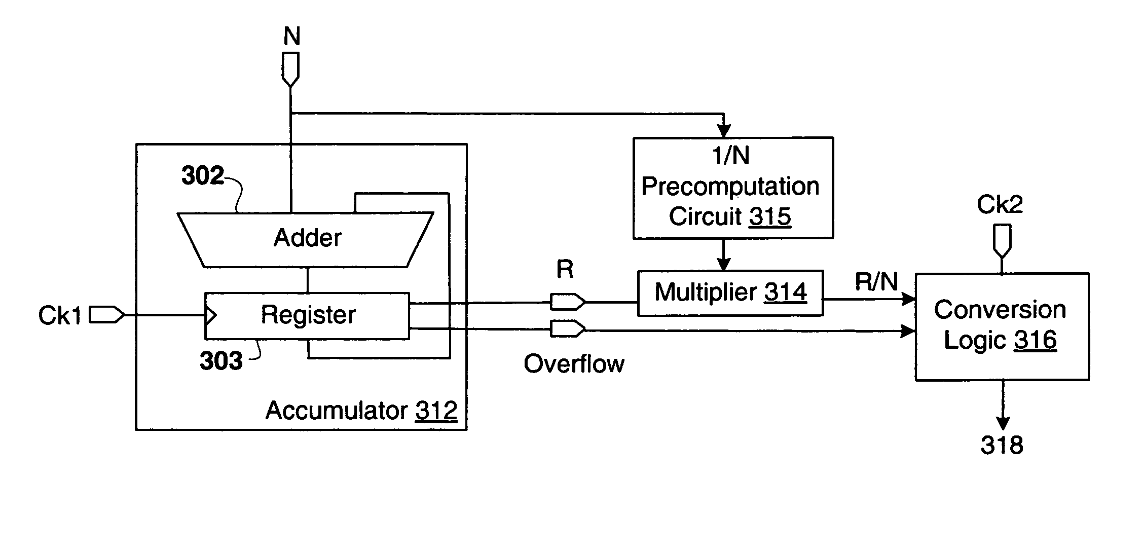
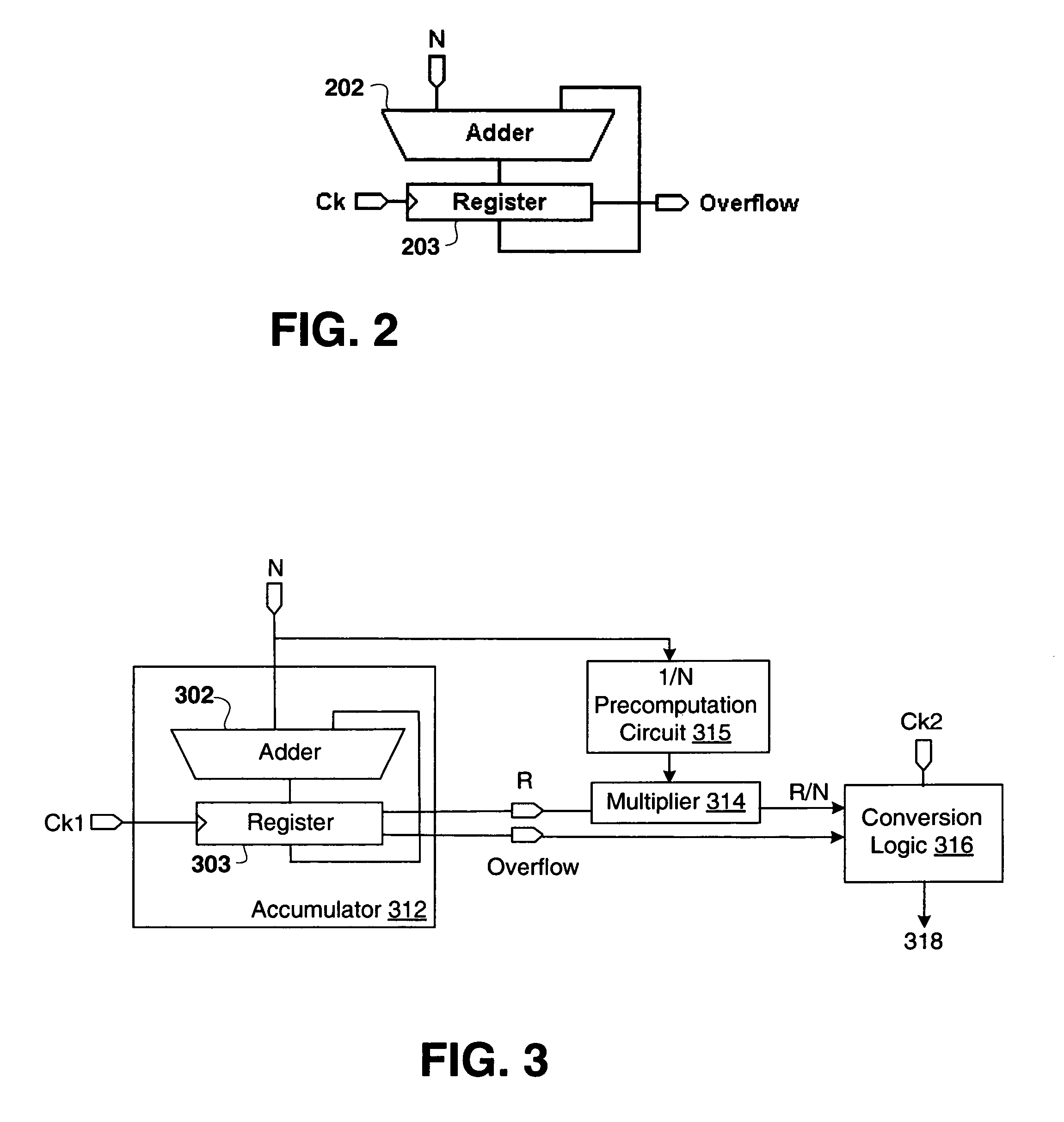
[0019]The accumulator circuitry and necessary logic for implementing embodiments of the present invention can be provided in a single FPGA. Although an FPGA is described as including such components, it is understood that either one or more other types of ICs can similarly include the components. Although other ICs can be used, for convenience, subsequent discussion of embodiments of the present invention will refer to components provided in an FPGA.

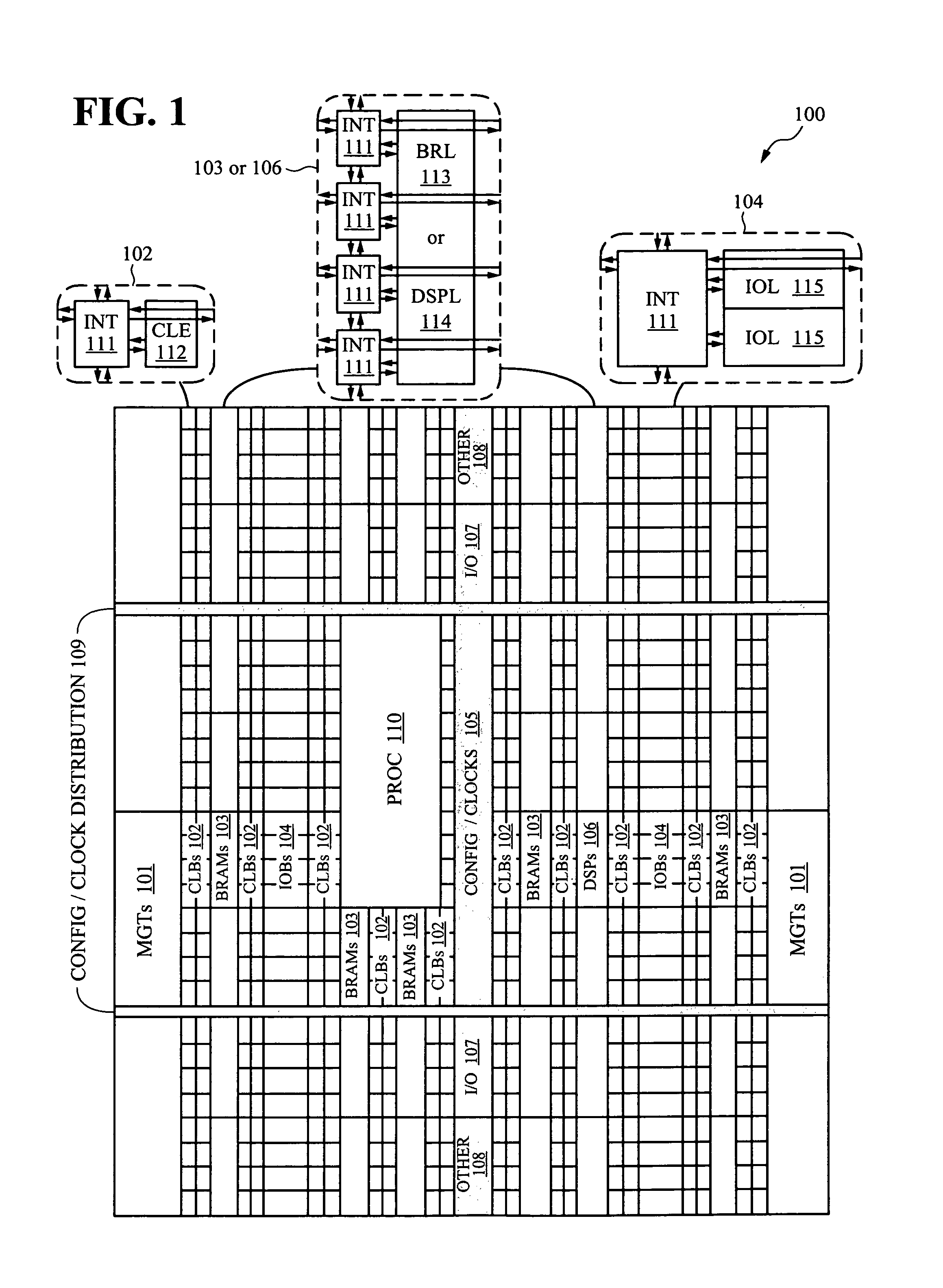
[0020]For reference, FIG. 1 illustrates one configuration of components that can be included in an FPGA. The components include a large number of different programmable tiles including multi-gigabit transceivers (MGTs 101), configurable logic blocks (CLBs 102), random access memory blocks (BRAMs 103), input / output blocks (IOBs 104), configuration and clocking logic (CONFIG / CLOCKS 105), digital signal processing blocks (DSPs 106), specialized input / output blocks (I / O 107) (e.g., configuration ports and clock ports), and other programmable...


PUM


Abstract

A direct digital synthesis is provided with added circuitry to reduce jitter in an IC so that a programmable frequency output can be provided near the limits of the IC system clock with minimal jitter. The system derives the quotient Q as a remainder R in an accumulator at the instant of an overflow, divided by a programmable input N. The quotient Q is subjected to conversion logic that can be provided by a fast parallel to serial converter such as, for example a multi-gigabit transceiver (MGT) of an FPGA. As an alternative to an MGT, a series of delay devices such as found in a carry chain can be used if calibration is performed to assure the accuracy of delays.

Description

BACKGROUND[0001]1. Technical Field[0002]The present invention relates to the use of Direct Digital Synthesis (“DDS”) or “phase accumulation” to provide a clock source with reduced jitter.[0003]2. Related Art[0004]If it is necessary to generate a programmable output frequency with fine resolution and low jitter, for example as a clock source for a digital circuit, there is a natural conflict between programmability and stability, i.e. between frequency granularity and jitter. DDS or “phase accumulation” is the well-known traditional method to perform this function.[0005]For DDS, an accumulator is clocked by the IC system clock, and overflow of the accumulator provides a digital pulse. The frequency of the pulse is related to the input to the accumulator. To program the frequency of overflow from the accumulator, a user selects the number added in the accumulator each clock cycle.[0006]DDS can generate an average frequency with high resolution, limited only by the length of the accumu...

Claims


Application Information

Patent Timeline
IPC IPC(8): G06F1/02
CPCG06F1/025G06F1/04
Inventor ALFKE, PETER H.
Owner XILINX INC
Why Eureka
Try Eureka