
Semiconductor device having open bit line architecture

a technology of open bit and semiconductor devices, applied in the field of semiconductor devices, can solve the problems of increasing the area of the memory cell array, complicated selection of i/o lines, and increasing the complexity of i/o lines selection

Active Publication Date: 2013-01-15
MICRON TECH INC
View PDF3 Cites 5 Cited by
  • Summary
  • Abstract
  • Description
  • Claims
  • Application Information

AI Technical Summary

Benefits of technology

The patent describes a semiconductor device that includes multiple memory mats. These memory mats can be selected based on different addresses. The invention allows for sharing a third memory mat between different areas of the device, which avoids complicated control logic and reduces the size of the memory cell field. The technical effect of this invention is improved efficiency and control logic in a semiconductor device that includes multiple memory mats.

Problems solved by technology

When the open bit line architecture is employed in such DRAMs, there occur problems that selection of I / O lines becomes complicated, an area of the memory cell array increases and the like.
As explained above, when the open bit line architecture is employed in a DRAM in which it is possible to switch I / O numbers, there are problems such that selection of I / O lines becomes complicated, or the area of the memory cell array increases.
These problems are not limited to DRAMs, but can occur to other semiconductor memory devices that employ the open bit line architecture, and can also occur to all semiconductor devices that include these devices.

Method used


Image

  • Semiconductor device having open bit line architecture
  • Semiconductor device having open bit line architecture
  • Semiconductor device having open bit line architecture

Examples


Embodiment Construction

[0035]Preferred embodiments of the present invention will be explained below in detail with reference to the accompanying drawings.

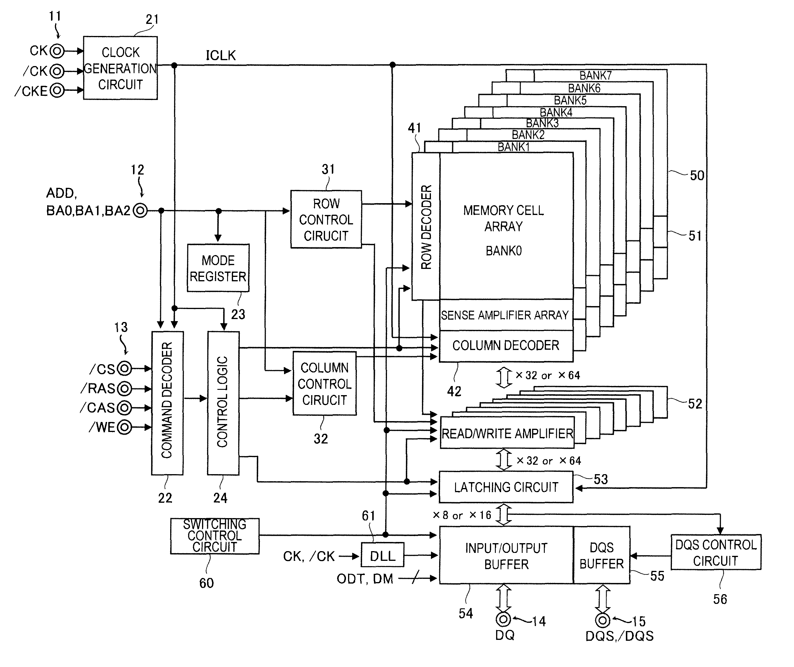
[0036]FIG. 1 is a block diagram showing a configuration of a semiconductor device according to an embodiment of the present invention.

[0037]The semiconductor device according to the present embodiment is a DDR2 synchronous DRAM (Synchronous Dynamic Random Access Memory) in which it is possible to set an I / O number to 8 bits or 16 bits. Because a prefetch number of the DDR2 synchronous DRAM is 4, when the I / O number is set to 8 bits, data of 32 bits is simultaneously input / output, and when the I / O number is set to 16 bits, data of 64 bits is simultaneously input / output.

[0038]The semiconductor device according to the present embodiment includes at least clock terminals 11, an address terminal 12, command terminals 13, a data input output terminal 14, and a data strobe terminal 15 as external terminals.

[0039]The clock terminals 11 are terminals to which clo...


PUM


Abstract

When an I / O number is 8 bit, a semiconductor device includes a first memory mat that is selected when X13 is (0) and X11 and X12 are (0, 0), a second memory mat that is selected when X13 is (1) and X11 and X12 are (0, 0), and a third memory mat that is selected irrespective of a value of X13 when X11 and X12 are (0, 0). When the I / O number is 16 bit, X13 is ignored, and the first to third memory mats are selected when X11 and X12 are (0, 0). In this manner, because the third memory mat is shared between so-called upper side and lower side, control is prevented from becoming complicated and an area is prevented from increasing.

Description

BACKGROUND OF THE INVENTION[0001]1. Field of the Invention[0002]The present invention relates to a semiconductor device, and more particularly relates to a semiconductor device including a memory cell array of an open bit line architecture.[0003]2. Description of Related Art[0004]In a DRAM (Dynamic Random Access Memory), which is a representative type of semiconductor memory devices, there has been known an open bit line architecture and a folded bit line architecture as methods for connecting a pair of bit lines to a sense amplifier. The open bit line architecture is a method in which a pair of bit lines connected to one sense amplifier is wired in mutually opposite directions with the sense amplifier sandwiched therebetween. Therefore, the pair of bit lines connected to the one sense amplifier is respectively allocated to a different memory mat. On the other hand, the folded bit line architecture is a method in which a pair of bit lines connected to one sense amplifier is wired in...

Claims


Application Information

Patent Timeline
Patent Type & Authority Patents(United States)
IPC IPC(8): G11C5/06
CPCG11C7/1069G11C7/1096G11C7/18G11C8/10G11C8/12G11C11/4087G11C11/4096G11C11/4097G11C7/1051G11C7/1078
Inventor NAKAOKA, YUJIICHIKAWA, HIROSHI
Owner MICRON TECH INC
Features
  • Generate Ideas
  • Intellectual Property
  • Life Sciences
  • Materials
  • Tech Scout
  • Unparalleled Data Quality
  • Higher Quality Content
  • 60% Fewer Hallucinations
Learn More