
Semiconductor device and semiconductor package including the same

a semiconductor and semiconductor technology, applied in the field of semiconductors, can solve the problems of reducing affecting the performance of the system, and reducing the efficiency of the system, so as to improve the layout and wiring, improve the efficiency of the substrate, and improve the effect of bias

Active Publication Date: 2013-01-29
SAMSUNG ELECTRONICS CO LTD
View PDF7 Cites 0 Cited by
  • Summary
  • Abstract
  • Description
  • Claims
  • Application Information

AI Technical Summary

Benefits of technology

Example embodiments describe a semiconductor device with an improved layout and wiring. This is achieved by efficiently providing a substrate and well bias voltage. These improvements enhance the design margin of wiring and provide reliable bias voltage. Furthermore, the patent text discusses a three-dimensional stack structure and semiconductor package that further improve design flexibility and bias voltage reliability.

Problems solved by technology

As the wiring gap decreases, providing power reliably and transmitting a signal correctly becomes more difficult, thereby a performance of a system is degraded.
As such, the smaller wiring gap becomes a limitation in increasing a degree of integration in a semiconductor device.

Method used


Image

  • Semiconductor device and semiconductor package including the same
  • Semiconductor device and semiconductor package including the same
  • Semiconductor device and semiconductor package including the same

Examples


Embodiment Construction

[0033]Various example embodiments will be described more fully with reference to the accompanying drawings, in which some example embodiments are shown. The present invention may, however, be embodied in many different forms and should not be construed as limited to example embodiments set forth herein. Rather, these embodiments are provided so that this disclosure will be thorough and complete, and will fully convey the scope of the present invention to those skilled in the art. Like reference numerals refer to like elements throughout this application.

[0034]It will be understood that, although the terms first, second, etc. may be used herein to describe various elements, these elements should not be limited by these terms. These terms are used to distinguish one element from another. For example, a first element could be termed a second element, and, similarly, a second element could be termed a first element, without departing from the scope of the present invention. As used here...


PUM

PropertyMeasurementUnit
bias voltageaaaaaaaaaa
bias voltagesaaaaaaaaaa
voltageaaaaaaaaaa

Abstract

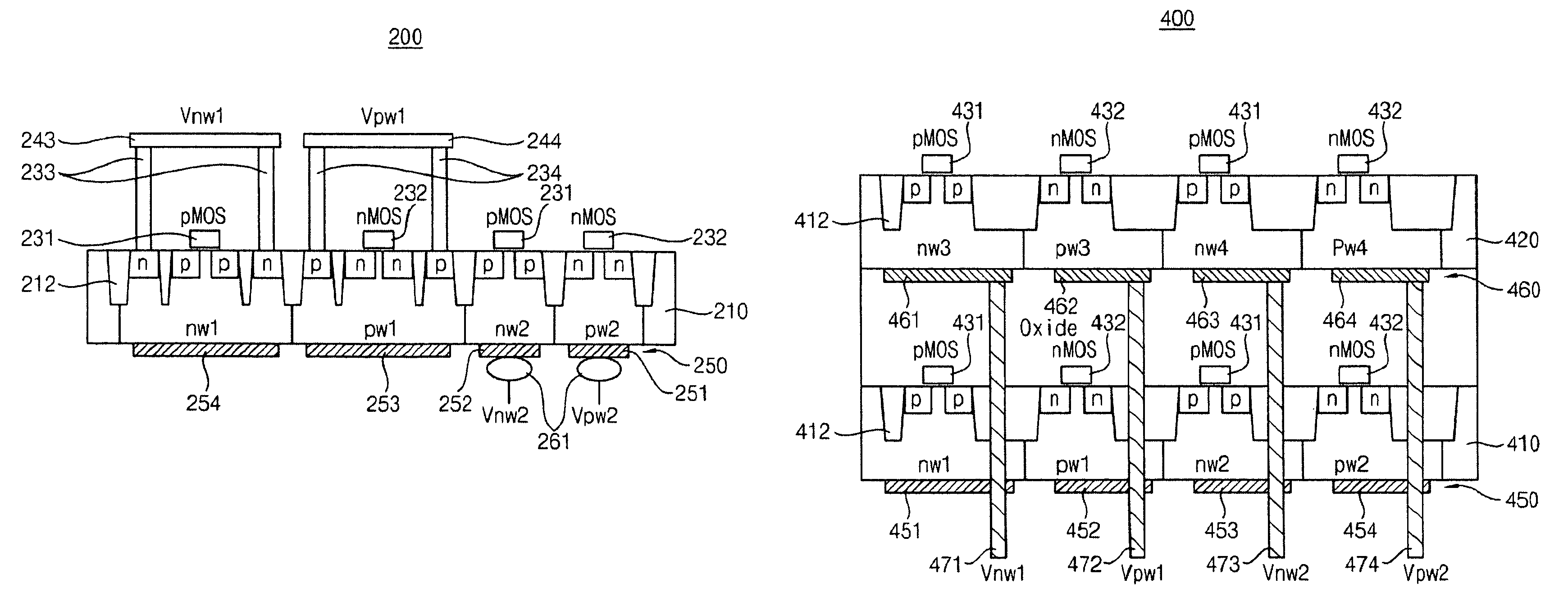
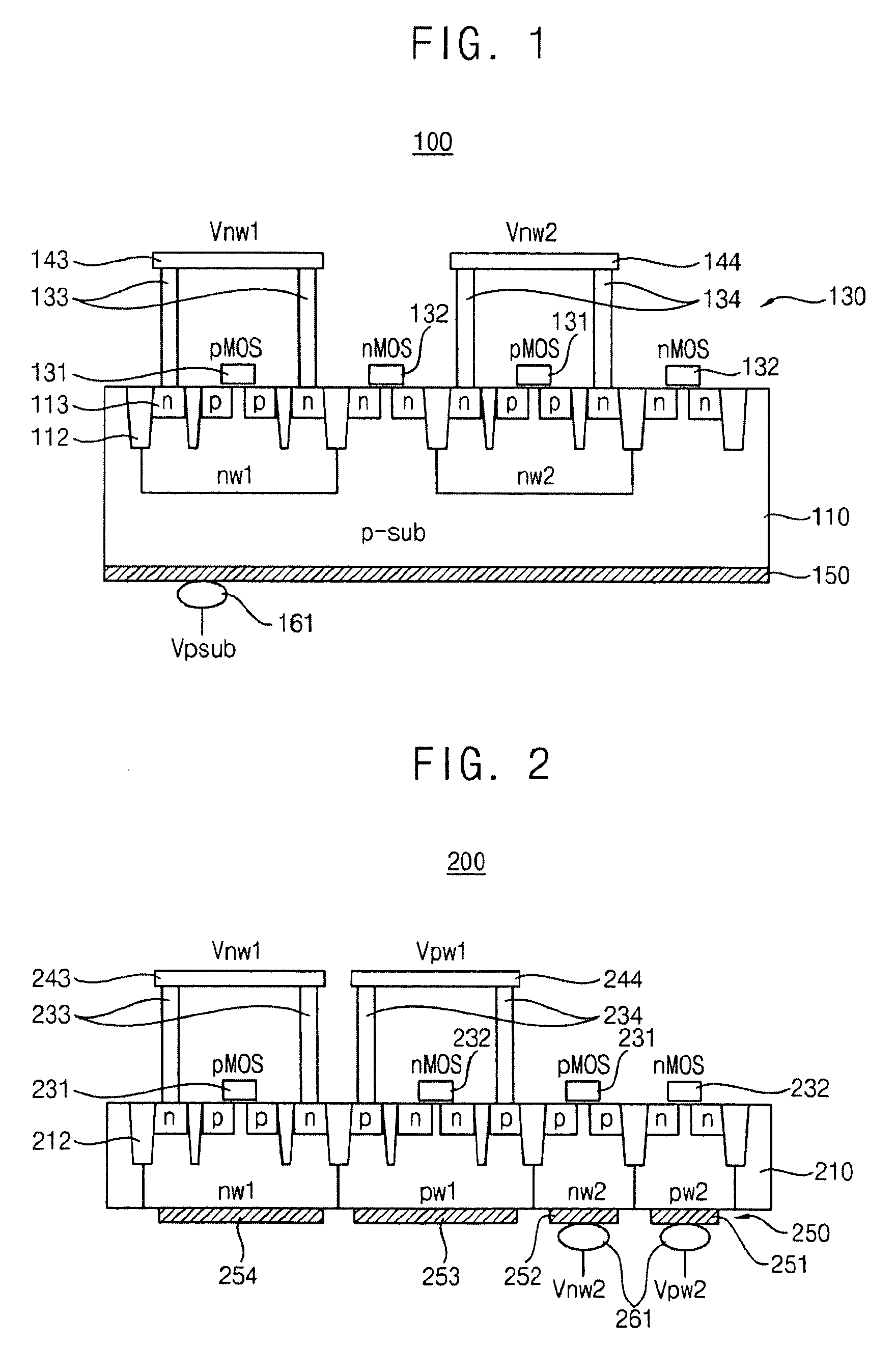
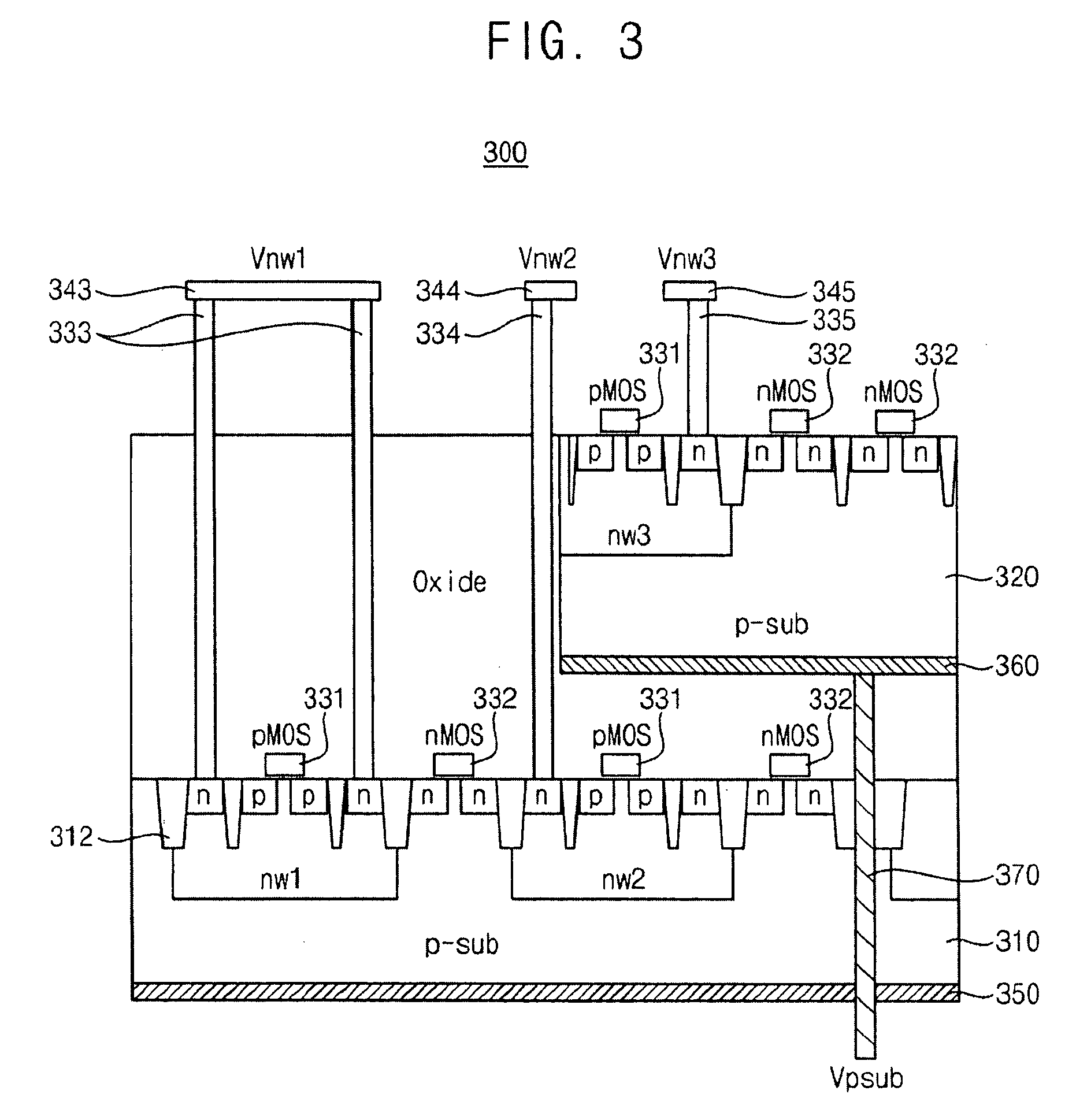
A semiconductor device includes a first substrate including at least one first well region and first impurity regions on portions of the substrate and a bias voltage plate on a surface of the substrate. A semiconductor device may be of a three dimensional stack structure, and in example embodiments, the semiconductor device may further include a through contact plug substantially perpendicularly penetrating at least one substrate and at least one bias voltage plate. Therefore, a design margin of a semiconductor device may be enhanced and a bias voltage may be provided reliably.

Description

PRIORITY STATEMENT[0001]This application claims priority under 35 USC §119 to Korean Patent Application No. 2008-0073664, filed on Jul. 28, 2008, in the Korean Intellectual Property Office (KIPO), the entire contents of which are herein incorporated by reference.BACKGROUND[0002]1. Technical Field[0003]Example embodiments relate to a semiconductor, and more particularly to a semiconductor device that enhances a design margin of wiring and reliably provides a substrate voltage and / or a well bias voltage, and a semiconductor package including the semiconductor device.[0004]2. Description of the Related Art[0005]As a degree of integration in a semiconductor device increases, a gap between wires for inputting and / or outputting a voltage signal or a current signal decreases. As the wiring gap decreases, providing power reliably and transmitting a signal correctly becomes more difficult, thereby a performance of a system is degraded. As such, the smaller wiring gap becomes a limitation in ...

Claims


Application Information

Patent Timeline
Patent Type & Authority Patents(United States)
IPC IPC(8): H01L27/108H10B12/00
CPCH01L23/481H01L25/0657H01L2224/48227H01L2225/06513H01L2225/06541H01L2924/01079H01L2924/3025H01L24/48H01L2224/73257H01L2924/00H01L2924/14H01L2924/181H01L2924/00014H01L2924/00012H01L2224/45099H01L2224/45015H01L2924/207H01L27/04
Inventor SONG, KI-WHANLEE, JUNG-BAE
Owner SAMSUNG ELECTRONICS CO LTD
Learn More