
Boost-forward-flyback high gain converter
a high gain converter and forward-flying technology, applied in the field of converters, can solve the problems of complex high gain converters, high cost, and inability to directly apply to renewable energy applications, and achieve the effects of reducing cost, simplifying voltage converting circuits, and improving voltage gain
- Summary
- Abstract
- Description
- Claims
- Application Information
AI Technical Summary
Benefits of technology
Problems solved by technology
Method used
Image

Examples
Embodiment Construction
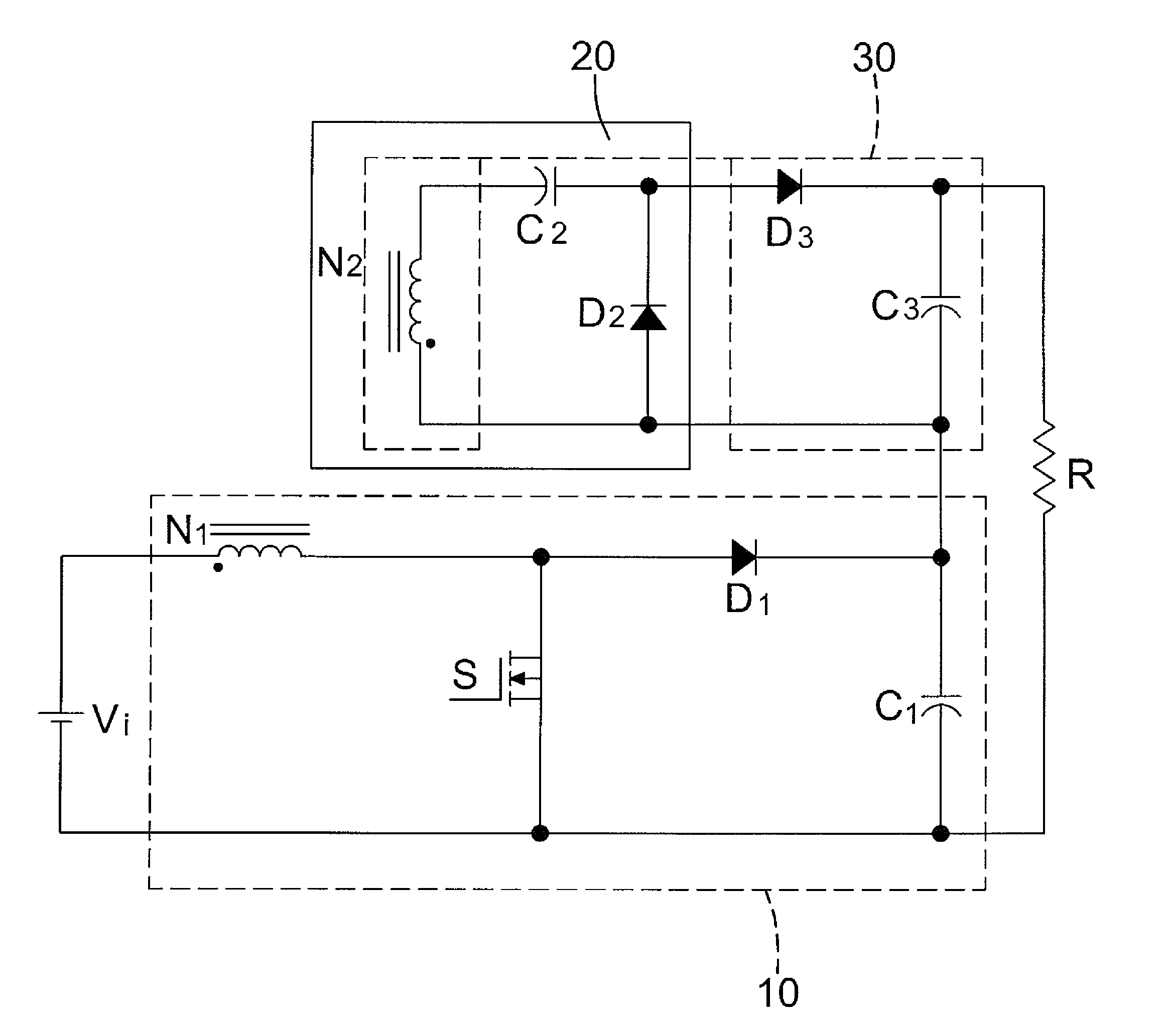
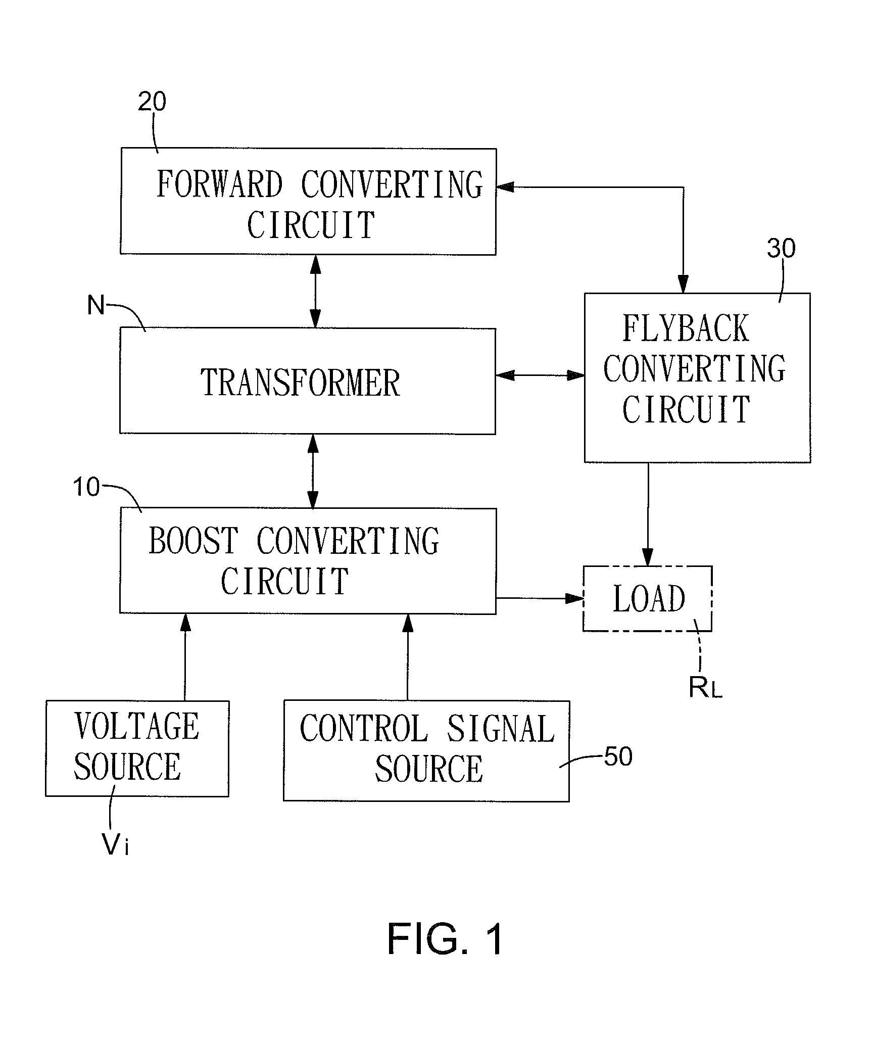
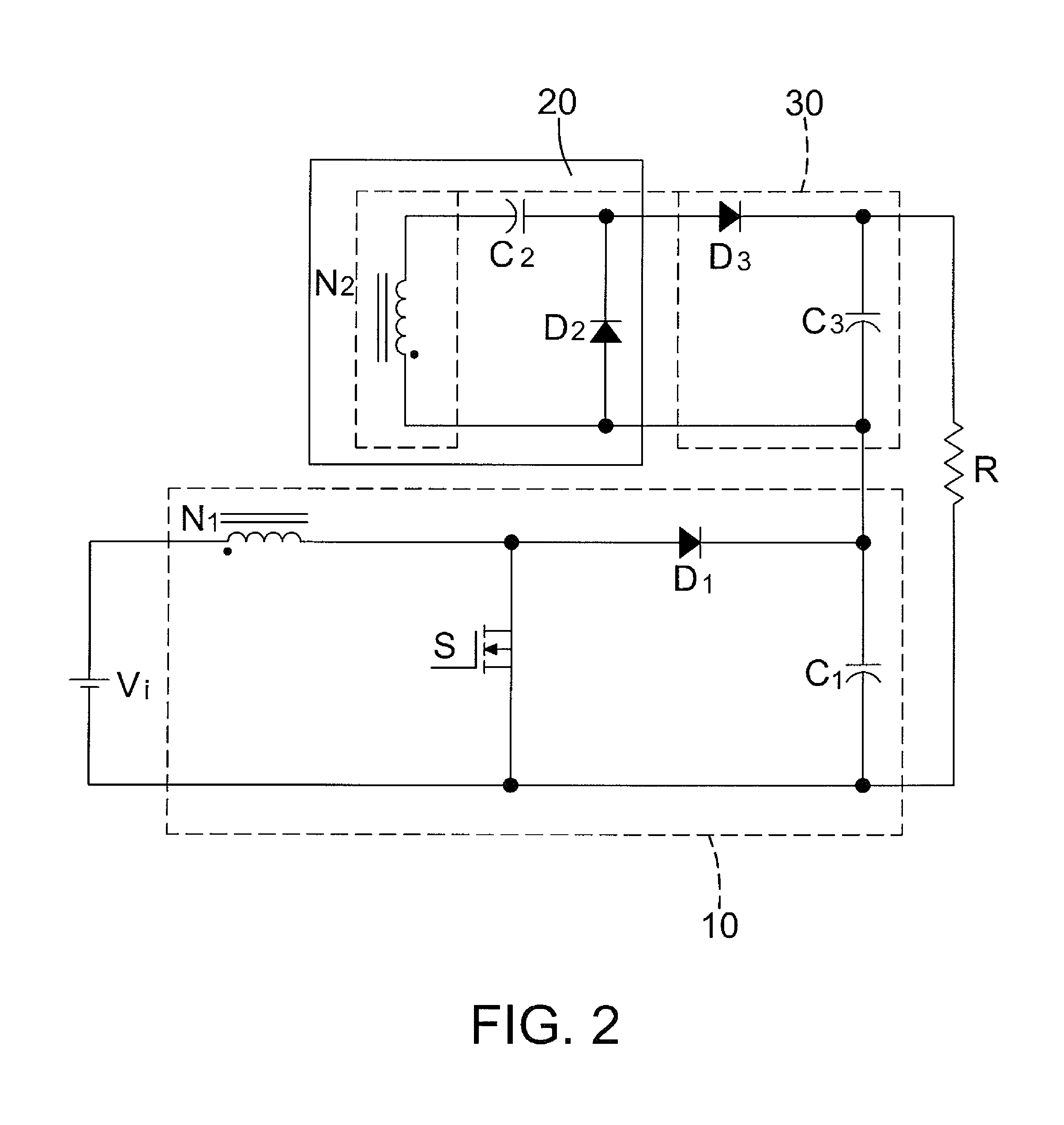
[0023]With reference to FIGS. 1 and 2, a boost-forward-flyback high gain converter in accordance with the present invention comprises a boost converting circuit (10), a forward converting circuit (20), a flyback converting circuit (30) and a transformer (N) and may be implemented in numerous embodiments depending on the implementation of the converting circuits (10, 20, 30) . . . .
[0024]The boost converting circuit (10) connects to an external voltage source (Vi) and an external control signal source (50) as inputs, is coupled to a load (RL) and comprises a switch (S), an input coil (N1), a boost diode (D1) and a boost capacitor (C1).
[0025]The control signal source (50) sends a control signal to the boost converting circuit (10) to activate voltage conversion between the voltage source (Vi) and the load (RL). The control signal source 50 may be a pulse width modulation (PWM) or the like.
[0026]The switch (S) may be a BJT, FET or the like, is connected to the control signal source (50...
PUM
 Abstract
Description
Claims
Application Information