Inductor built-in boost unit converter

A technology of converters and inductors, which is applied in the field of boost unit converters with built-in inductors. It can solve the problems of large number of components, difficult gain, complex circuit structure, etc., and achieve high conversion efficiency, large voltage gain, and simple circuit structure. Effect

CN107659144AActive
4 Cites 10 Cited by

Patent Information

Authority / Receiving Office
CN · China
Patent Type
Applications(China)

Smart Images

  • Figure 1
    Figure 1
  • Figure 2
    Figure 2
Patent Text Reader

Abstract

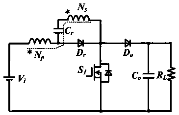
The invention relates to an inductor built-in boost unit converter, belonging to the technical field of power electronic converters. The inductor built-in boost unit converter comprises an inductor built-in boost unit, a direct-current voltage source, a power switch tube, an output power diode and a filter capacitor, wherein the inductor built-in boost unit comprises a coupling inductor, an energystorage capacitor and a freewheel diode. By the invention, the voltage gain can be increased to a relatively high level, the defect that a conventional Boost circuit is insufficient in boost capacityis overcome, and the inductor built-in boost unit converter has the advantages of high gain, simple structure and high conversion efficiency. Compared with an existing coupling inductor boost circuit, it is unnecessary to add extra leakage inductance energy absorption and switch tube clamping circuits, the inductor built-in boost unit converter has the simplest circuit structure and the minimum components, and the conversion efficiency and the reliability are higher.
Need to check novelty before this filing date? Find Prior Art

Description

technical field

[0001] The invention relates to the field of power electronic converters, in particular to a converter with a built-in inductance boost unit. Background technique

[0002] In many low-input, high-output voltage applications such as new energy power generation, industrial and mining lighting, and automotive electronics, high-gain converters are required for voltage conversion. The theoretical output gain of the traditional Boost converter can reach infinity, but in practice, due to the existence of parasitic parameters, the actual gain is difficult to exceed and the conversion efficiency is low. The traditional coupled inductor boost circuit needs to add passive or active clamping The circuit is used to absorb the leakage inductance energy and suppress the voltage peak of the switching tube. The circuit structure is complex and the number of components is large. Therefore, it is necessary to design a converter with an inductance built-in boost unit that does n...

Examples

Embodiment Construction

[0014] Below in conjunction with accompanying drawing and specific embodiment the present invention is described in further detail:

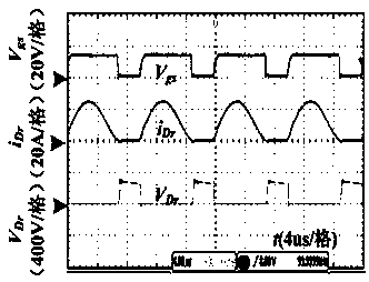
[0015] The invention provides a boost unit converter circuit with an inductance built in to realize high-gain and high-efficiency power conversion. The built-in boost unit of the inductance can realize the increase of the gain, and under the condition that the leakage inductance of the coupling inductor and the resonance period of the energy storage capacitor must be less than the conduction time of the power switch tube, it can realize the zero-current turn-off of the freewheeling diode to improve the conversion efficiency.

[0016] Such as figure 1 The converter with a built-in inductance step-up unit shown includes a built-in inductance step-up unit, a DC voltage source V in , power switch tube S1, output diode D o , filter capacitor C O and load R L , characterized in that: the DC voltage source V in It is connected with the input end o...