Shower plate, method for manufacturing the shower plate, plasma processing apparatus using the shower plate, plasma processing method and electronic device manufacturing method
a technology for shower plates and plasma processing equipment, which is applied in the field of shower plate manufacturing methods, plasma processing methods and electronic device manufacturing methods, can solve the problems of difficult to perform a uniform process over the whole surface of the substrate to be processed with a high processing rate, uneven plasma formation by a conventional plasma processing apparatus, and limited area with high electron density, etc., to achieve uniform and efficient plasma excitation and microwave degradation
- Summary
- Abstract
- Description
- Claims
- Application Information
AI Technical Summary
Benefits of technology
Problems solved by technology
Method used
Image

Examples
first embodiment
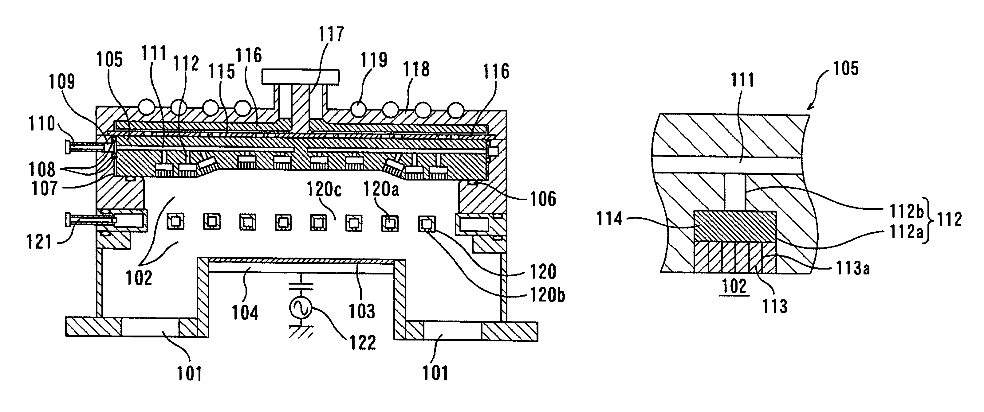
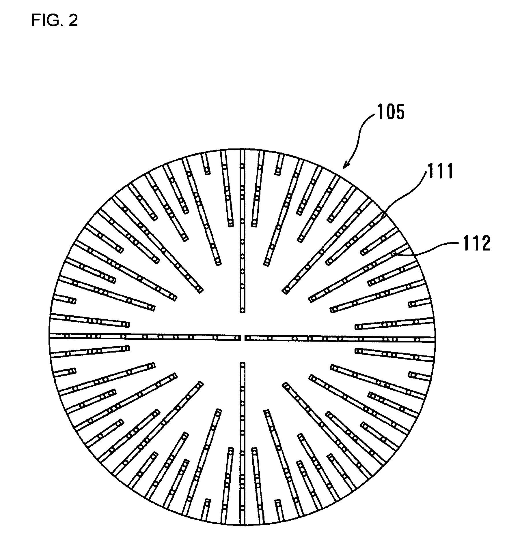
[0041]FIG. 1 illustrates a first embodiment of the present invention. A microwave plasma processing apparatus is illustrated in FIG. 1. An illustrated microwave plasma processing apparatus has a processing chamber 102 in which gas is exhausted via a plurality of exhaust ports 101. In the processing chamber 102, a holding member 104 for holding a substrate to be processed 103 is arranged. In order to uniformly exhaust gas of the processing chamber 102, the processing chamber 102 defines a ring shaped space to the circumference of the holding member 104. The plurality of exhaust ports 101 is arranged in regular intervals to communicate with space, namely, they are arranged in axial symmetry against the substrate to be processed 103. By an arrangement of these exhaust ports 101, gas in the processing chamber 102 can be exhausted more uniformly through the exhaust ports 101.
[0042]A shower plate 105 is fixed onto the upper section of the processing chamber 102 via O-ring for seals 106 at...
second embodiment
[0068]A second embodiment of the present invention is shown in FIG. 5. Referring to FIG. 5, a microwave plasma processing apparatus is shown. The same symbols are attached to the portions, which overlap with the first embodiment, and the explanation will be omitted.
[0069]In this example, in the upper portion of the processing chamber 102, a plate-shaped shower plate 201 is attached via O-ring for seals 106 as a part of outer wall of processing chamber 102 in the position corresponding to the substrate to be processed 103 on the holding member 104. A large number of openings (230 pieces), namely, longitudinal holes 200, have been formed on the plate-shaped shower plate 201. The plate-shaped shower plate 201 is structured by the alumina having a relative permittivity of 9.8 and low microwave dielectric loss (dielectric loss is 1×10⁻⁴ or lower). Further, in the processing chamber 102, a cover plate 202, which is formed of alumina, is attached onto the upper surface side of the shower p...
third embodiment
[0078]A third embodiment of the present invention is shown in FIG. 10. A microwave plasma processing apparatus is shown in FIG. 10. The same symbols are attached to the portions, which overlap with the first and the second embodiments, and the explanation will be omitted. A longitudinal hole 300 of a shower plate 301 in this example is having structure as shown in FIG. 11. That is, a gas discharge hole 300a, 0.05 mm in diameter and 0.5 mm in length, has been opened in the processing chamber 102 side where plasma is excited. The gas introduction side of the gas discharge hole 300a is connected to a hole 300b having diameter of 1 mm. In order to avoid electric field concentration of microwave, a chamfering processing 303 is given to the corner of gas introduction side of the hole 300b. And a sintered porous-ceramic body 302 having a cylindrical shape of height of 5 mm and having a pore that communicates in the gas flow direction is fixed onto the bottom section of the hole 300b having...
PUM
| Property | Measurement | Unit |
|---|---|---|
| pore diameter | aaaaa | aaaaa |
| bending strength | aaaaa | aaaaa |
| diameter | aaaaa | aaaaa |
Abstract
Description
Claims
Application Information
 - R&D
- Intellectual Property
- Life Sciences
- Materials
- Tech Scout
- Unparalleled Data Quality
- Higher Quality Content
- 60% Fewer Hallucinations
Browse by: Latest US Patents, China's latest patents, Technical Efficacy Thesaurus, Application Domain, Technology Topic, Popular Technical Reports.
© 2025 PatSnap. All rights reserved.Legal|Privacy policy|Modern Slavery Act Transparency Statement|Sitemap|About US| Contact US: help@patsnap.com