Clock control signal generation circuit, clock selector, and data processing device

a clock selector and signal generation circuit technology, applied in the direction of generating/distributing signals, pulse techniques, instruments, etc., can solve the problems of obstructing factors, affecting the effect of power consumption reduction, and a great deal of time lost as standby tim

Inactive Publication Date: 2013-02-12
RENESAS ELECTRONICS CORP
View PDF10 Cites 14 Cited by
  • Summary
  • Abstract
  • Description
  • Claims
  • Application Information

AI Technical Summary

Benefits of technology

[0009]On the assumption that the microcomputer system returns from the power-saving mode for 32-kHz clock operation to the high-speed-operation mode for 100-MHz clock operation, a standby time representing the time of 6250 cycles of the clock after switching is expected to be created at the switching from the 32-kHz clock to the 100-MHz clock in a conventional clock selector, as described above. The standby time can cause a serious malfunction in an application to e.g. a controller such that the practicability of real-time processing is a key requirement. In addition, the operating time of a high-frequency clock generator like PLL, which consumes a large power, is made longer, which is considered to be an obstacle to achieving the reduction of power consumption.
[0011]According to JP-A-2004-166194, a hedge circuit which involves the use of a high-speed reference clock and is separately prepared, is provided in parallel with a cascaded structure of latch circuits different from each other in logic for detection. As to the hedge circuit like this, the same number of the hedge circuits as the number of clocks are required. Therefore, the increase in the number of clocks is expected to increase the circuit scale.
[0018]The first effect is that a technique for switching between clock signals having different frequencies at a high speed can be provided. The second effect is that it is possible to achieve a high-speed switching between clocks having different frequencies with no increase in the circuit scale.

Problems solved by technology

In light of the time of one cycle of the high-frequency clock after switching, the fact implies that a great deal of time will be lost as a standby time.
Therefore, a processing time of a process using a low-frequency clock is considered to make an obstructive factor to the speedup of clock switching.
The standby time can cause a serious malfunction in an application to e.g. a controller such that the practicability of real-time processing is a key requirement.
In addition, the operating time of a high-frequency clock generator like PLL, which consumes a large power, is made longer, which is considered to be an obstacle to achieving the reduction of power consumption.

Method used


Image

  • Clock control signal generation circuit, clock selector, and data processing device
  • Clock control signal generation circuit, clock selector, and data processing device
  • Clock control signal generation circuit, clock selector, and data processing device

Examples


first embodiment

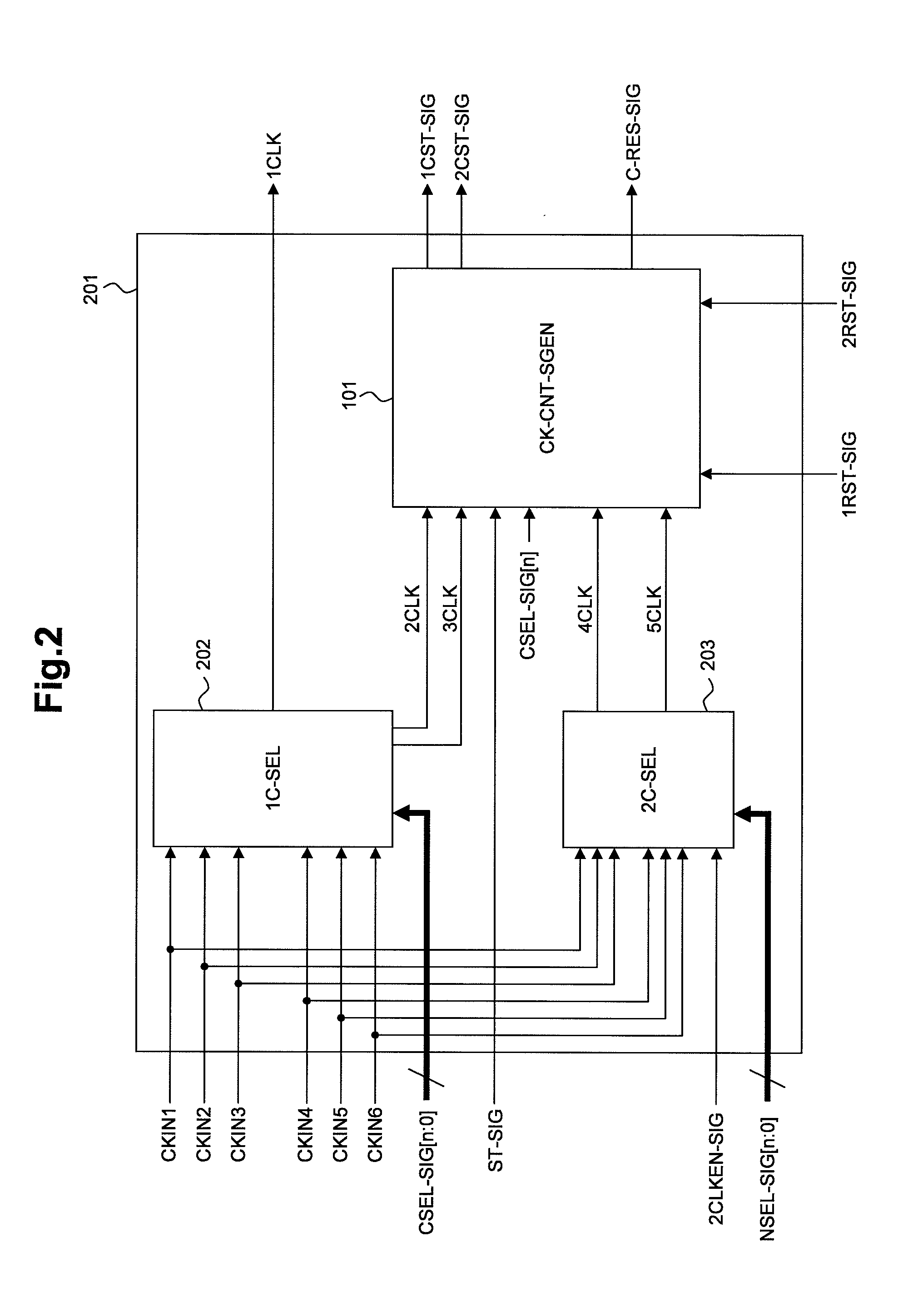
[0096]FIG. 2 shows an example of the configuration of a modification of the clock-control-signal-generation circuit 101. The clock-control-signal-generation circuit shown in FIG. 2 has a first clock-select unit (1C-SEL) 202 and a second clock-select unit (2C-SEL) 203 in addition to the clock-control-signal-generation circuit (CK-CNT-SGEN) 101, which has been described in connection with the From this, the clock-control-signal-generation circuit shown in FIG. 2 shall be herein referred to as “select-type clock-control-signal-generation circuit 201”.

[0097]The select-type clock-control-signal-generation circuit 201 accepts inputs of: a plurality of clock signals, i.e. input clock signals CKIN1 to CKIN6; a current-select signal CSEL-SIG[n:0] of n+1 bits (n is a positive integer); a new-select signal NSEL-SIG[n:0] of n+1 bits; a switching-trigger signal ST-SIG; a second clock-select-unit-enable signal 2CLKEN-SIG; a first reset signal 1RST-SIG; and a second reset signal 2RST-SIG. The sel...

second embodiment

[0108]The clock selector 301 shown in FIG. 3 has: the select-type clock-control-signal-generation circuit (SCC-GEN) 201, which has been described in connection with the second embodiment; a gating control unit (G-CNT) 302; a clock-gating unit (C-GAT) 303; a first select-signal-holding unit (1SEL-ST) 304; a second select-signal-holding unit (2SEL-ST) 305; and a reset-signal-generation unit (REST-GEN) 306.

[0109]The clock selector 301 accepts inputs of: a plurality of clock signals (input clock signals CKIN1 to CKIN6); a clock-select signal of n+1 bits; a switching-trigger signal ST-SIG; and a second clock-select-unit-enable signal 2CLKEN-SIG. Also, the clock selector 301 outputs: an output clock signal CKOUT; a current-select signal CSEL-SIG[n:0] of n+1 bits; a switching-run signal SEL-RUN-SIG; and a second reset signal 2RST-SIG.

[0110]The clock-select signal of n+1 bits serves to indicate, to the clock selector 301, which of the input clock signals CKIN1 to CKIN6 to select and output....

third embodiment

[0113]The gating control unit 302 makes nonactive and outputs the first gating-control signal 1GAT-SIG on condition that the first clock-stop-permission signal 1CST-SIG is active, and the clock-resume-permission signal C-RES-SIG is nonactive. Also, the gating control unit 302 makes nonactive and outputs the second gating-control signal 2GAT-SIG on condition that the second clock-stop-permission signal 2CST-SIG is active, and the clock-resume-permission signal C-RES-SIG is nonactive. Now, it is noted that in the third embodiment, only one of the first gating-control signal 1GAT-SIG and the second gating-control signal 2GAT-SIG is made nonactive; the first and second gating-control signals are never rendered nonactive concurrently.

[0114]The clock-gating unit 303 outputs an output clock signal CKOUT with its logic level fixed at Low on condition that the first gating-control signal 1GAT-SIG is nonactive, whereas on condition that the second gating-control signal 2GAT-SIG is nonactive, ...


PUM


Abstract

Provided are a technique for high-speed switching between clock signals different in frequency, and a clock-control-signal-generation circuit which serves to generate a control signal for clock switching in a clock selector operable to switch between clock signals including a first clock signal based on first and second clock-stop-permission signals and a clock-resume-permission signal. The clock-control-signal-generation circuit includes: a before-switching clock processing unit; and an after-switching clock processing unit. In each of the before-and after-switching clock processing units, the high-frequency clock processing subunit and the low-frequency clock processing subunit take partial charges of processing of clock signals involved in the switching respectively, whereby the processing is speeded up.

Description

CLAIM OF PRIORITY[0001]The Present application claims priority from Japanese application JP 2010-042771 filed on Feb. 26, 2010, the content of which is hereby incorporated by reference into this application.FIELD OF THE INVENTION[0002]The present invention relates to a clock-control-signal-generation circuit operable to generate a signal for controlling a clock signal, a clock selector operable to select, from among clock signals out of synchronization with each other, one clock signal, and output the select one, and a data processor including the clock-control-signal-generation circuit and clock selector.BACKGROUND OF THE INVENTION[0003]Japanese Unexamined Patent Publication No. JP-A-2007-86960 discloses a clock-switching circuit which can switch a clock without generating a hazard and a collapse of duty rate. The clock-switching circuit has: a first synchronizing circuit for synchronizing a clock-select signal by a first clock; a second synchronizing circuit for synchronizing the ...

Claims


Application Information

Patent Timeline
Patent Type & Authority Patents(United States)
IPC IPC(8): H04L7/00G01R31/28
CPCG06F1/08
Inventor NARA, YOSHIKAZUTAKAHASHI, YASUHIKO
Owner RENESAS ELECTRONICS CORP
Why Eureka
Try Eureka