Optical information recording medium and recording/reproducing method therefor
a technology of optical information and recording medium, which is applied in the direction of instruments, photomechanical devices, transportation and packaging, etc., can solve the problems of low modulation degree in the case of performing recording and small number of replayable times, and achieve excellent sensitivity and reaction speed, and ensure the margin of manufacture process. , the effect of simple manufacturing process
- Summary
- Abstract
- Description
- Claims
- Application Information
AI Technical Summary
Benefits of technology
Problems solved by technology
Method used
Image
Examples
example 1
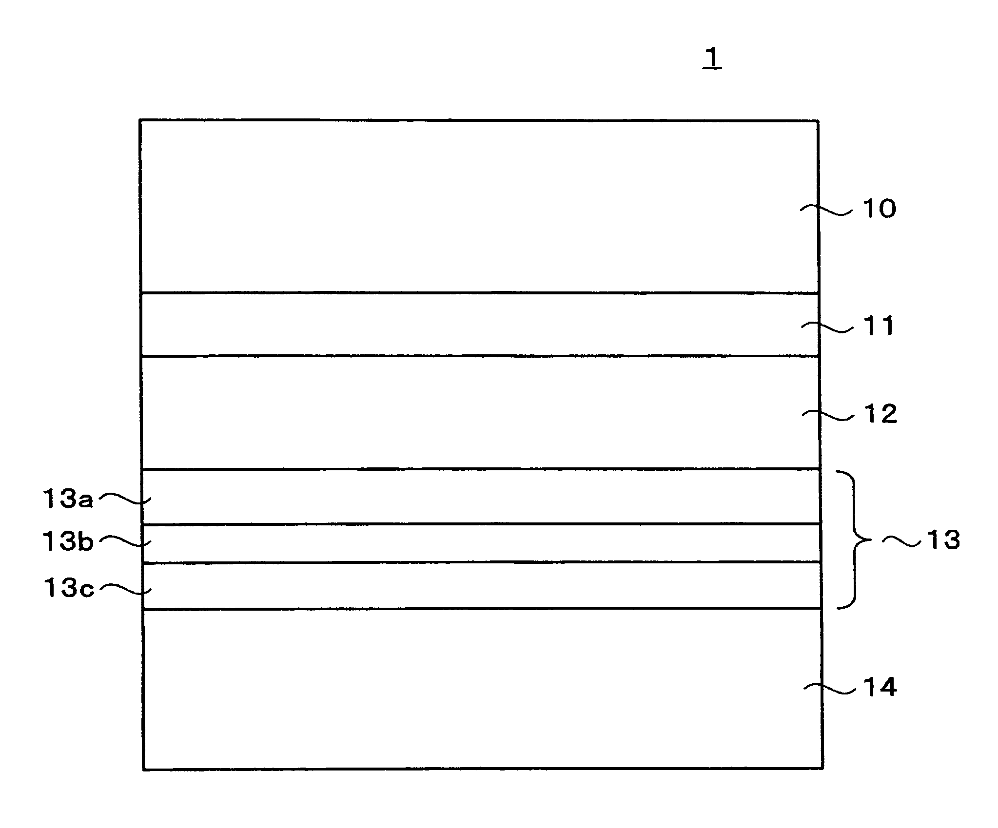
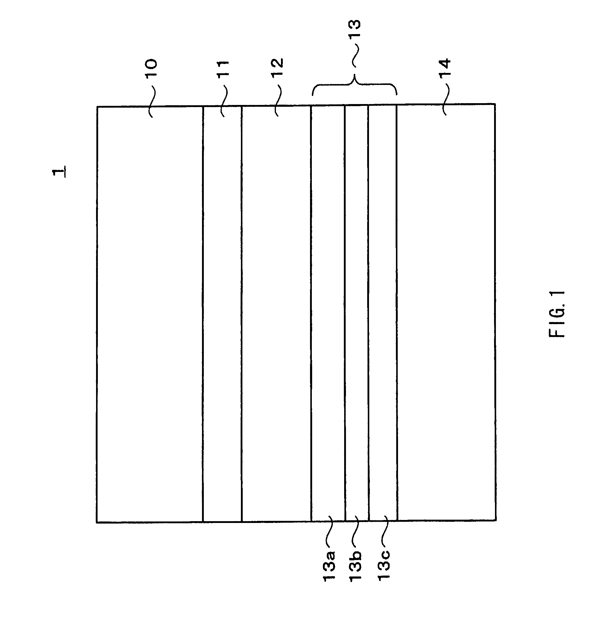
[0057]The optical information recording medium 1 for performing recording and reproduction by an optical disk recording / reproducing apparatus using a two-group objective lens having a numerical aperture of 0.85 and a semiconductor laser source that emits a laser beam having a wavelength of 405 nm was manufactured as follows.
[0058]As the substrate 10, a polycarbonate substrate having a thickness of 1.1 mm and having a groove with a track pitch of 0.32 μM on one side was manufactured by injection molding. The first information recording layer 11 was formed on the polycarbonate substrate. An adhesive of an ultraviolet curable type was coated on the first information recording layer 11 to a thickness of 25 μm by spin coating. A groove track was transferred by a stamper made of polycarbonate. The adhesive was irradiated with ultraviolet light to form the intermediate layer 12. On the intermediate layer 12, a Ta2O5 film having a thickness of 10 nm as the first dielectric layer 13a, the re...
example 2
[0082]The optical information recording medium 2 for performing recording and reproduction by an optical disk recording / reproducing apparatus using a two-group objective lens having a numerical aperture of 0.85 and a semiconductor laser source that emits a beam having a wavelength of 405 nm was manufactured as follows.
[0083]As the substrate 20, a polycarbonate substrate having a thickness of 1.1 mm and having a groove with a track pitch of 0.32 μm on one side was manufactured by injection molding. The first information recording layer 11 was formed on the polycarbonate substrate. The first intermediate layer 22 having a thickness of 15 μm was formed by the method described in Example 1 on the first recording layer 11. On the first intermediate layer 22, a Ta2O5 film having a thickness of 10 nm as the first dielectric layer 23a, the recording layer 23b having a thickness of 7 nm, and a Ta2O5 film having a thickness of 26 nm as the second dielectric layer 23c were sequentially formed ...
PUM
| Property | Measurement | Unit |
|---|---|---|
| thickness | aaaaa | aaaaa |
| wavelength | aaaaa | aaaaa |
| wavelength range | aaaaa | aaaaa |
Abstract
Description
Claims
Application Information


