Electro-optic displays, and materials and methods for production thereof

a technology of optical displays and optical displays, applied in the field of optical displays, can solve the problems of inadequate service life of optical displays, preventing their widespread use, and gas-based electrophoretic media appearing to be susceptible to the same types of problems

Active Publication Date: 2013-03-05
E INK CORPORATION
View PDF313 Cites 51 Cited by
  • Summary
  • Abstract
  • Description
  • Claims
  • Application Information

AI Technical Summary

Benefits of technology

[0076]In a second main aspect, this invention provides an article of manufacture (a “detachable tab front plane laminate” or “DTFPL”) for use in the production of an electro-optic display, the article comprising a conductive layer and a layer of electro-optic medium, the conductive layer having a main section covered by the layer of electro-optic medium, an exposed section in at least part of which the conductive layer is exposed free from the electro-optic medium, and a weak section connecting the main section and the exposed section, such that the exposed section can be manipulated to cause rupture of the weak section, thereby separating the exposed section from the main section without substantial damage to the main section.
[0077]Typically, in the detachable tab front plane laminate of the present invention, all sections of the conductive layer will be supported on a supporting layer (for example, a polymeric film) and both the conductive layer and supporting layer will have weak sections to enable the exposed section of the conductive layer and the associated part of the supporting layer to be detached from the main section of the conductive layer and the associated part of the supporting layer. The supporting layer may also serve other functions, for example by acting as a barrier against water vapor and / or ultra-violet radiation, and / or providing a desired surface texture.
[0079]As described above, typically a front plane laminate intended for testing will have two separate conductive layers, one conductive layer (P112 in FIG. 2) being that which will form the front electrode in the final display, and the other conductive layer (P118 in FIG. 2) being part of a conductive release sheet which will be removed from the front plane laminate before lamination to a backplane. Desirably, in such a dual conductive layer front plane laminate, a detachable exposed section is provided for each conductive layer. In order to facilitate removal of the two separate detachable exposed sections, they are desirably offset from one another, i.e., spaced from one another in the plane of the layer of electro-optic medium. The exposed section of the front electrode conductive layer may be provided as illustrated in the same way as in FIG. 2, that is to say by providing an aperture extending through layers of the front plane laminate (and the conductive release sheet, if the conductive release sheet covers the location of the aperture) overlying the front electrode conductive layer. As in FIG. 2, the portion of the front electrode conductive layer exposed by the aperture may be strengthened by providing a conductive pad in electrical contact with the conductive layer. Although the exposed sections of the two conductive layers could reside on the same detachable tab, it will typically be convenient to provide two separate detachable tabs for the exposed sections of the two conductive layers. As discussed in more detail below, providing separate tabs has the advantage that, at least in some cases, the exposed section of the conductive layer on the release sheet can be provided simply by weakening the appropriate area of the FPL and then removing from the relevant tab the front substrate, with the electro-optic medium and adhesive attached thereto.
[0087]thereafter, manipulating the exposed section to cause rupture of the weak section, thereby separating the exposed section from the main section without substantial damage to the main section.

Problems solved by technology

Nevertheless, problems with the long-term image quality of these displays have prevented their widespread usage.
For example, particles that make up electrophoretic displays tend to settle, resulting in inadequate service-life for these displays.
Such gas-based electrophoretic media appear to be susceptible to the same types of problems due to particle settling as liquid-based electrophoretic media, when the media are used in an orientation which permits such settling, for example in a sign where the medium is disposed in a vertical plane.
Indeed, particle settling appears to be a more serious problem in gas-based electrophoretic media than in liquid-based ones, since the lower viscosity of gaseous suspending fluids as compared with liquid ones allows more rapid settling of the electrophoretic particles.
However, the methods used for assembling LCD's cannot be used with solid electro-optic displays.
This LCD assembly process cannot readily be transferred to solid electro-optic displays.
Electro-optic displays are often costly; for example, the cost of the color LCD found in a portable computer is typically a substantial fraction of the entire cost of the computer.
However, this method of forming connections tends to be undesirable from a manufacturing point of view, since the placement of the connections is of course a function of the backplane design, so that FPL coated with a specific arrangement of gutters can only be used with one, or a limited range of backplanes, whereas for economic reasons it is desirable to produce only one form of FPL which can be used with any backplane.
However, such removal of electro-optic medium poses its own problems, especially when the FPL is formed by coating a thin (less than about 25 μm) polymeric film.
Typically, the electro-optic medium must be removed by the use of solvents or mechanical cleaning, either of which may result in damage to, or removal of, the electrically-conductive layer of the FPL (this electrically-conductive layer usually being a layer of a metal oxide, for example indium tin oxide, less than 1 μm thick), causing a failed electrical connection.
In extreme cases, damage may also be caused to the front substrate (typically a polymeric film) which is used to support and mechanically protect the conductive layer.
In some cases, the materials from which the electro-optic medium is formed may not be easily solvated, and it may not be possible to remove them without the use of aggressive solvents and / or high mechanical pressures, either of which will exacerbate the aforementioned problems.
Also, depending upon the location of the connection, bending of the electrically-conductive layer and the associated front substrate may crack the conductive layer, resulting in failure to make a proper connection between the backplane and the conductive layer, and hence display failure.
However, when the prior art FPL structure shown in FIGS. 1 and 2 is based upon a PET layer having a thickness of about 1 mil (25 μm), there is a risk of mechanical damage to the aperture P122 or the adjacent parts of the silver layer P124 and ITO layer P112, and since in this structure the apertures P122 are used both for testing purposes and as the top plane connections in the final display, any damage to the apertures or the adjacent conductive layers during testing may affect the performance of the final display.
Such laser cutting may damage the silver layer P124 and / or the adjacent part of the ITO layer P112, with the disadvantageous results already noted.
Moreover, the structure shown in FIGS. 1 and 2 requires that the same top plane connections (apertures P122) be used for both testing and in the final display, whereas for engineering reasons it may be more convenient to provide separate sets of top plane connections for the two purposes, and leaves the inner tab sections P104A remaining on the final FPL after the conductive release sheet P118 / P120 has been removed, and in some cases the presence of these protruding inner tab sections P104A may be inconvenient.

Method used


Image

  • Electro-optic displays, and materials and methods for production thereof
  • Electro-optic displays, and materials and methods for production thereof
  • Electro-optic displays, and materials and methods for production thereof

Examples


Embodiment Construction

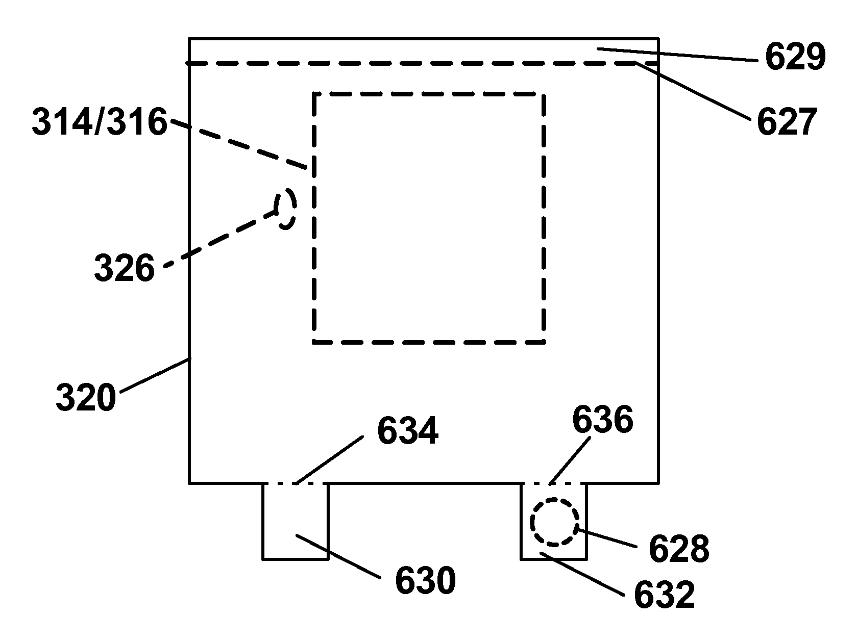
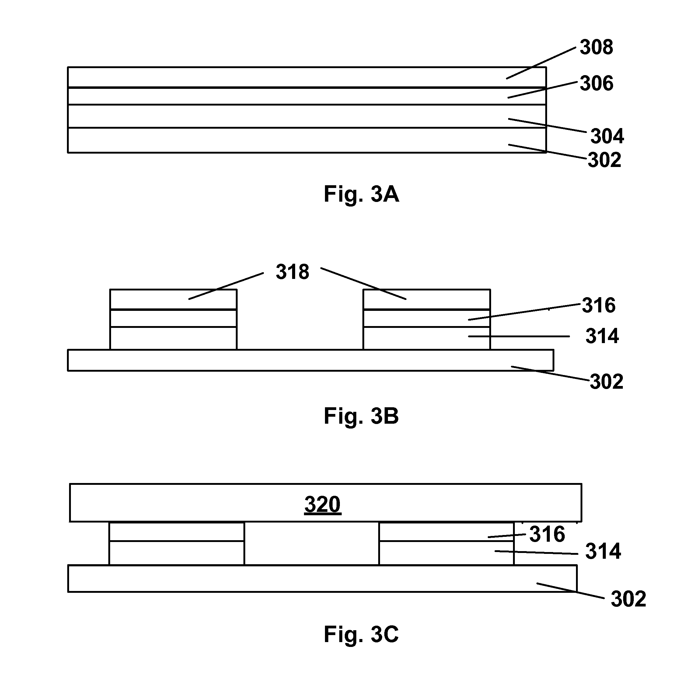
[0098]Before describing in detail various embodiments of the present invention it is useful to set out certain definitions. The term “backplane” is used herein consistent with its conventional meaning in the art of electro-optic displays and in the aforementioned patents and published applications, to mean a rigid or flexible material provided with one or more electrodes. The backplane may also be provided with electronics for addressing the display, or such electronics may be provided in a unit separate from the backplane. In flexible displays (and the present invention is especially although not exclusively intended for use in flexible displays), it is highly desirable that the backplane provide sufficient barrier properties to preventingress of moisture and other contaminants through the non-viewing side of the display. If one or more additional layers need to be added to the backplane to reduce ingress of moisture and other contaminants, the barrier layers should be located as c...


PUM

PropertyMeasurementUnit
diameteraaaaaaaaaa
thicknessaaaaaaaaaa
thicknessaaaaaaaaaa

Abstract

A sub-assembly useful in an electro-optic display includes a conductive layer and a layer of electro-optic medium. The conductive layer has a main section covered by the electro-optic medium, an exposed section free from the electro-optic medium, and a weak section connecting the main section and the exposed section, so that the exposed section can be manipulated to rupture the weak section, thus separating the exposed section from the main section without substantial damage.

Description

REFERENCE TO RELATED APPLICATIONS[0001]This application claims benefit of Provisional Applications Nos. 60 / 946,997 and 60 / 947,001, both filed Jun. 29, 2007. This application is also a continuation-in-part of application Ser. No. 11 / 682,409, filed Mar. 6, 2007 (Publication No. 2007 / 0211331, now U.S. Pat. No. 7,733,554), which itself claims benefit of Provisional Application No. 60 / 767,171, filed Mar. 8, 2006.[0002]This application is also related to:[0003](a) U.S. Pat. No. 6,982,178;[0004](b) application Ser. No. 10 / 605,024, filed Sep. 2, 2003 (Publication No. 2004 / 0155857, now U.S. Pat. No. 7,561,324);[0005](c) U.S. Pat. No. 7,110,164;[0006](d) U.S. Pat. No. 7,075,703;[0007](e) application Ser. No. 11 / 550,114 filed Oct. 17, 2006 (Publication No. 2007 / 0109219, now U.S. Pat. No. 7,839,564);[0008](f) application Ser. No. 11 / 612,732, filed Dec. 19, 2006 (Publication No. 2007 / 0152956, now U.S. Pat. No. 7,649,674); and[0009](g) application Ser. No. 11 / 850,831, filed Sep. 6, 2007 (Publicat...

Claims


Application Information

Patent Timeline
Patent Type & Authority Patents(United States)
IPC IPC(8): G01R31/02G01R23/17G02B26/00G02F1/167
CPCG02B26/026G02F1/167G02F2202/28
Inventor DANNER, GUY M.ALBERT, JONATHAN D.NORTHROP, VALERIE C.WONG, TIMOTHY L.
Owner E INK CORPORATION
Why Eureka
Try Eureka