Electric contact member

a technology of contact member and carbon film, which is applied in the direction of connection contact member material, conductor, instruments, etc., can solve the problems of low adhesiveness between a base material and carbon film, low reactivity of film, and difficulty in obtaining good adhesion, etc., and achieve good adhesiveness

Active Publication Date: 2013-04-02
KOBE STEEL LTD +1
View PDF11 Cites 2 Cited by
  • Summary
  • Abstract
  • Description
  • Claims
  • Application Information

AI Technical Summary

Benefits of technology

[0009]However, the contact probe pin on which the carbon film is formed has a problem of low adhesiveness between a base material and the carbon film. The carbon film has low reactivity to the base material composed of a usual metal, so that it is difficult to obtain good adhesion. Further, it has been considered to be the cause of decreased adhesiveness that the carbon film generally has a low thermal expansion coefficient compared to the metal base material. That is to say, when the temperature is raised when forming the film, the film does not follow contraction of the base material due to the difference in thermal expansion therebetween. Accordingly, compressive stress remains in the film, resulting in a state where the film is easily peeled off.
[0010]In order to improve adhesion between the film and the base material, various solutions are also exemplified in the above-mentioned patent documents. For example, the above-mentioned JP-A-10-226874 shows a method of reducing internal stress of a carbon film, and JP-A-2002-318247 proposes a stepwise gradient composition layer between a carbon film and a base metal. Further, JP-A-2003-231203 exemplifies an intermediate layer such as a metal or nitride (for example, CrN) layer, and JP-A-2007-24613 exemplifies in its example to form an intermediate layer having a gradient composition comprising Cr film / Cr, graphite and W, thereby improving adhesion between a carbon film and a base material.
[0026]According to the electric contact member of the invention, a carbon film comprising a metal and / or a carbide thereof is formed on a surface of an underlying layer comprising Au, Au alloy, Pd or Pd alloy, with the interposition of an intermediate layer having a predetermined lamination structure, thereby being able to form the carbon film on a surface of a base material with good adhesiveness. Thus, the electric contact member that can keep stable electric contact over a long period of time has been realized.

Problems solved by technology

However, the contact probe pin on which the carbon film is formed has a problem of low adhesiveness between a base material and the carbon film.
The carbon film has low reactivity to the base material composed of a usual metal, so that it is difficult to obtain good adhesion.
Further, it has been considered to be the cause of decreased adhesiveness that the carbon film generally has a low thermal expansion coefficient compared to the metal base material.
However, Au or Pd has low reactivity, and any technique for improving adhesiveness, particularly taking into account an underlying layer composed of such a material, has not hitherto been proposed, in an actual state.

Method used


Image

  • Electric contact member
  • Electric contact member
  • Electric contact member

Examples


example 1

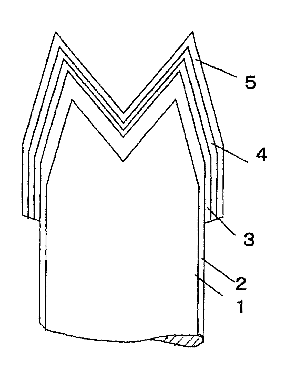
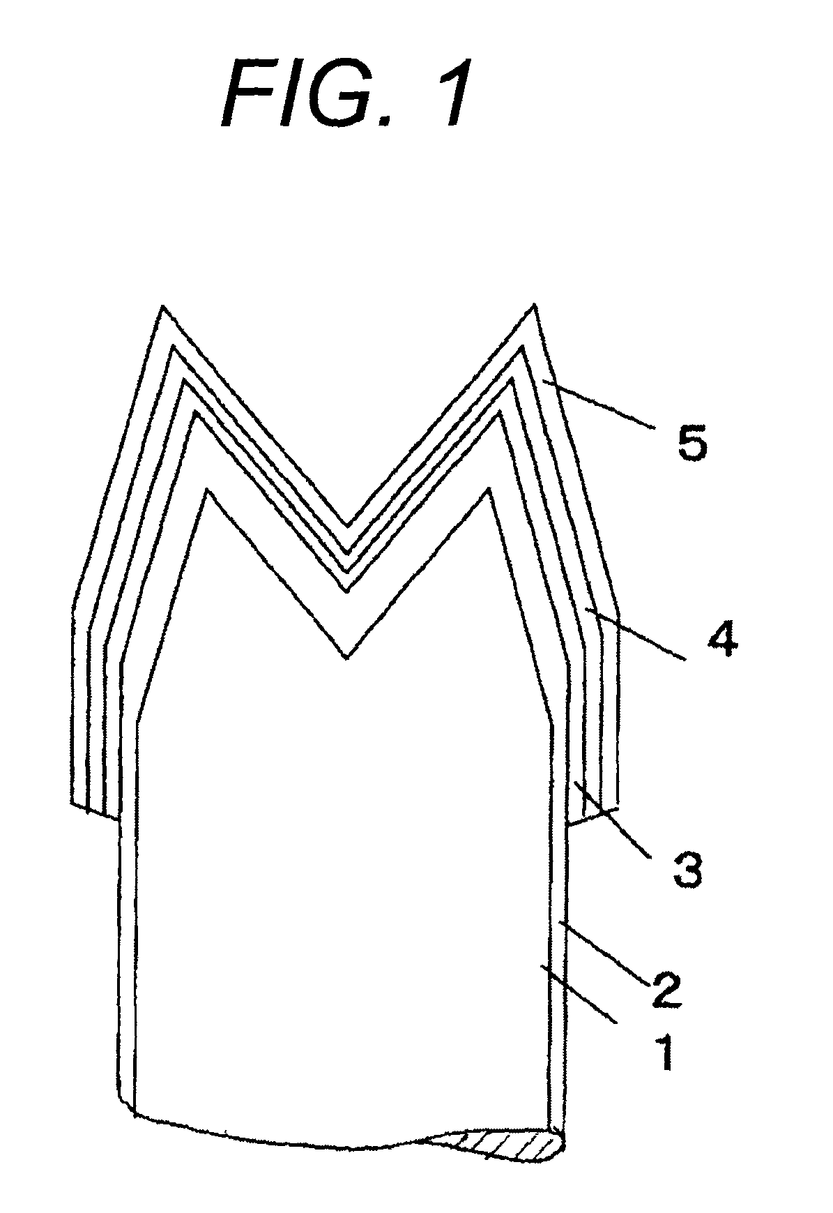
[0076]A spring built-in probe with a tip part divided into four parts as shown in FIG. 1 was used as a contact probe pin. This contact probe pin was Au-plated on a surface thereof, and a base material 1 was made of Be—Cu. Incidentally, FIG. 1 schematically shows a state where the tip part is projected from the side, and the shape thereof is shown as two projections. Further, in FIG. 1, reference numeral 2 indicates an underlying layer, reference numeral 3 indicates an inner layer composed of Ni or Ni alloy, reference numeral 4 indicates an outer layer comprising at least one of Cr, Cr alloy, W and W alloy, and reference numeral 5 indicates a carbon film comprising a metal and / or a carbide thereof.

[0077]A carbon (graphite) target, a Cr target and a Ni target were each arranged in a magnetron sputtering chamber, and the contact probe pin was arranged in a position opposed to them.

[0078]After inside of the sputtering chamber was evacuated down to 6.7×10⁻⁴ Pa or less, Ar gas was introdu...

example 2

[0084]A contact probe pin with a carbon film was prepared by forming, in turn, a Ni layer, Cr layer, gradient composition layer and a carbon film in the same manner as in Example 1 with the exception that a contact probe pin (having a tip part divided into four parts as with Example 1) in which Pd (an underlying layer) was plated on the surface of the base material 1 made of Be—Cu was used.

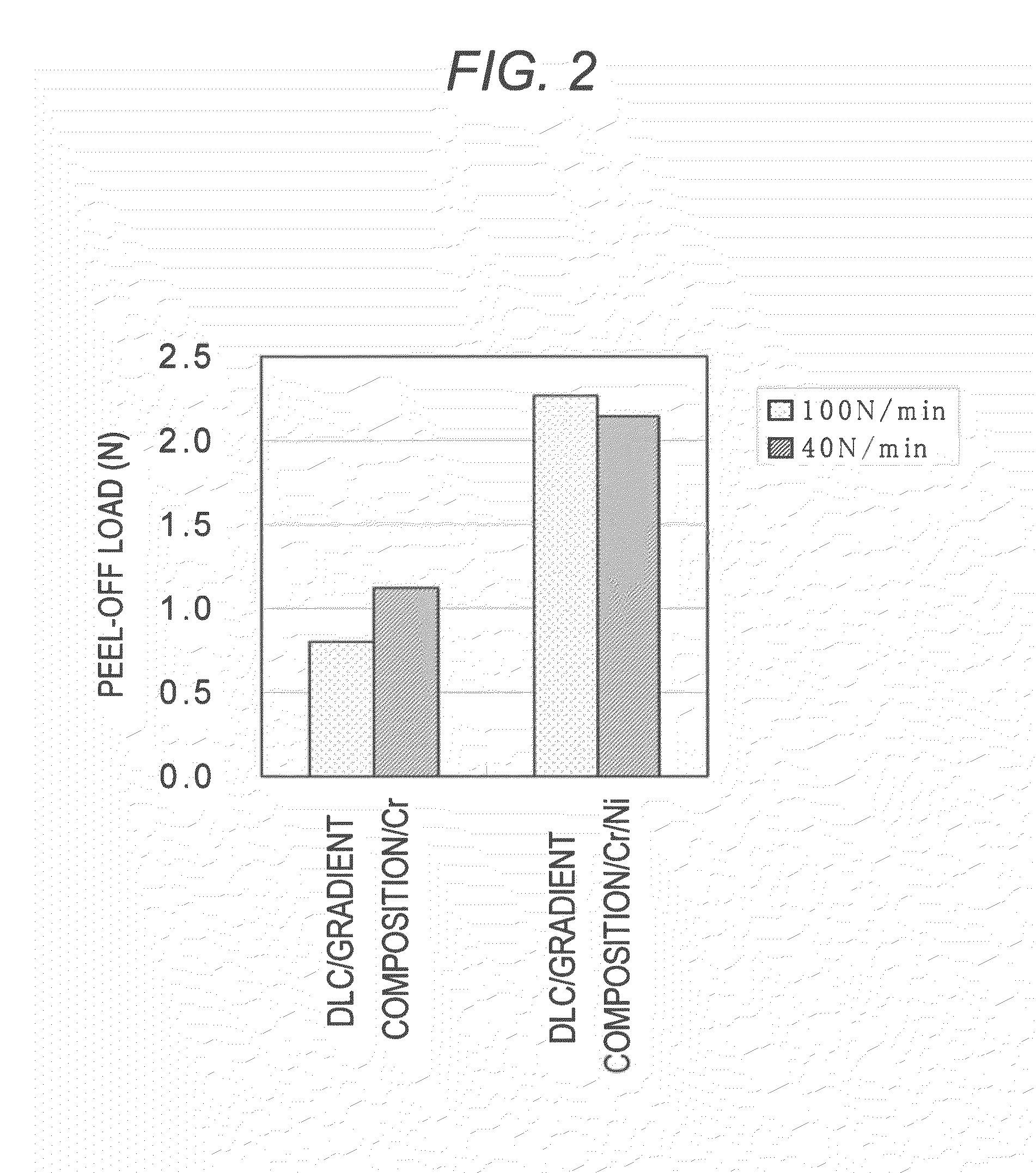
[0085]Using the contact probe pin with a carbon film formed above, contact were performed 100,000 times to an electrode composed of lead-free solder (Sn+3 atomic % Cu+0.5 atomic % Ag), and the state of film peel-off of the tip part was observed, and in order to confirm the presence or absence of stability of the electric resistance value due to film peel-off, a current of 100 mA was turned on for each contact, and changes in electric resistance (changes in resistance) were determined (however, the measurement of the resistance was made once pre 100 times). Changes in electric resistance (the relat...

example 3

[0086]A contact probe pin with a carbon film was prepared by forming, in turn, a Ni layer, Cr layer, gradient composition layer and a carbon film in the same manner as in Example 1 with the exception that a commercially available contact probe pin in which the base material 1 is a Pd alloy (having a tip part divided into four parts as with Example 1) was used.

[0087]Using the contact probe pin with a carbon film formed above, contact was performed 100,000 times to an electrode composed of lead-free solder (Sn+3 atomic % Cu+0.5 atomic % Ag), and the state of film peel-off of the tip part was observed. As a result, film peel-off was not observed, and it was confirmed that an adhesiveness of a stable film could be secured as with Example 2.


PUM

PropertyMeasurementUnit
thicknessaaaaaaaaaa
contact resistanceaaaaaaaaaa

Abstract

Provided is an electric contact member which reduces, to the utmost, peel-off of a carbon film that is caused at the time of use of the electric contact member having at least an edge to keep stable electric contact over a long period of time. Disclosed is an electric contact member which repeatedly contacts with a device under test at a tip part of the electric contact member in which the tip part has an edge, the electric contact member comprising: a base material; an underlying layer comprising Au, Au alloy, Pd or Pd alloy, which is formed on a surface of the base material of the tip part; an intermediate layer which is formed on a surface of the underlying layer; and a carbon film comprising at least one of a metal and a carbide thereof which is formed on a surface of the intermediate layer, wherein the intermediate layer has a lamination structure comprising: an inner layer comprising Ni or Ni alloy; and an outer layer comprising at least one of Cr, Cr alloy, W and W alloy.

Description

CROSS-REFERENCE TO RELATED APPLICATIONS[0001]This application claims priority from Japanese Patent Application No. 2009-228057 filed on Sep. 30, 2009, the entire subject matter of which is incorporated herein by reference.BACKGROUND OF THE INVENTION[0002]1. Field of the Invention[0003]The present invention relates to an electric contact member that is used for inspection of electric properties of a semiconductor element and repeatedly contacts with an electrode at a tip part of the electric contact member in which the tip part has an edge, and particularly to an electric contact member having excellent durability, which is not deteriorated in conductivity by repeated inspection. Incidentally, the electric contact member of the invention typically includes a contact probe (contact probe pin) formed in a pin shape (needle shape), but also includes, for example, one in a leaf spring shape and one in other shapes. In short, any electric contact member is included, as long as it repeated...

Claims


Application Information

Patent Timeline
Patent Type & Authority Patents(United States)
IPC IPC(8): H01B5/00
CPCH01B5/00G01R1/06738G01R1/06761H01R13/03
Inventor HIRANO, TAKAYUKIYAMAGUCHI, AKASHIMIYAMOTO, TAKASHI
Owner KOBE STEEL LTD
Why Eureka
Try Eureka