ESD protection device and manufacturing method therefor

a protection device and manufacturing method technology, applied in the direction of overvoltage protection resistors, spark plugs, spark gap details, etc., can solve the problems of increased variation in product characteristics, difficult to provide high-reliability products, and difficult to create paths

Active Publication Date: 2013-04-16
MURATA MFG CO LTD
View PDF9 Cites 9 Cited by
  • Summary
  • Abstract
  • Description
  • Claims
  • Application Information

AI Technical Summary

Benefits of technology

[0019]In the ESD protection device according to a preferred embodiment of the present invention, the metallic particles are preferably Cu particles. This is because the use of Cu particles as the metallic particles makes it possible to constitute an ESD protection device which is able to lower the discharge starting voltage and the peak voltage.
[0020]Furthermore, silicon carbide particles are preferably used as the semiconductor particles. This is because the use of silicon carbide particles as the semiconductor particles makes it possible to lower the clamp voltage.
[0021]In addition, in the ESD protection device according to a preferred embodiment of the present invention, when the vitreous material is produced by a reaction between the metallic particles and the semiconductor particles, a discharge auxiliary electrode with the vitreous material dispersed uniformly can be formed efficiently even with certainty, without the need to add any glass component separately to the raw material.
[0022]In addition, when the ESD protection device is configured to cause the cavity section provided in the ceramic base material to face the discharge gap section where the opposed electrode on one side and the opposed electrode on the other side, which constitute the opposed electrodes, have portions opposed to each other, and a region of the discharge auxiliary electrode located on the discharge gap section, a discharge phenomenon is also produced in the cavity section during ESD application, thus significantly allowing the discharge capacity to be improved more than in the absence of the cavity section.
[0023]Furthermore, the method for manufacturing an ESD protection device according to another preferred embodiment of the present invention includes the steps of printing, on one principal surface of a first ceramic green sheet, a discharge auxiliary electrode paste including metallic particles with an average particle diameter of about 1.0 μm or more, semiconductor particles, and an organic vehicle, at least one of the metallic particles and the semiconductor particles including, on surfaces thereof, a network-forming component of glass, and a combination of the metallic particles and the semiconductor particles having a ratio of about 7 volume % to about 25 volume %, thereby forming an unfired discharge auxiliary electrode; printing an opposed electrode paste, thereby forming unfired opposed electrodes provided with an opposed electrode on one side and an opposed electrode on the other side, the opposed electrodes each partially covering the discharge auxiliary electrode, and the opposed electrodes being arranged with a distance therebetween; stacking a second ceramic green sheet on one principal surface of the first ceramic green sheet, thereby forming an unfired laminated body; and firing the laminated body to react surfaces of the metallic particles of the discharge auxiliary electrode with surfaces of the semiconductor particles, thereby producing a vitreous material. Thus, the method allows an ESD protection device including the structure according to a preferred embodiment of the present invention to be manufactured efficiently even with certainty.
[0026]In addition, when alumina-coated Cu particles are used as the metallic particles included in the discharge auxiliary electrode, whereas silicon carbide particles are used as a raw material for the semiconductor particles, the alumina (Al2O3), a minute amount of silicon oxide which will be typically present on the surface of the silicon carbide, etc., can serve as the network-forming component of the glass to provide bonding through the vitreous material between the metallic particles, between the semiconductor particles, or between the metallic particles and the semiconductor particles for constituting the discharge auxiliary electrode, thereby allowing the efficient manufacture of an ESD protection device which has stable characteristics, and undergoes no characteristic degradation even when static electricity is applied repeatedly.

Problems solved by technology

In addition, miniaturization in design with an increase in signal frequency has made it difficult to create paths, and LSI itself has been highly sensitive to static electricity.
However, in the case of this overvoltage protection element, the addition of the adhesive (glass) is essential, and there is thus a possibility that the following problems will be caused.
There is a tendency for variation in product characteristics to be increased due to defective dispersion of the glass, and it is difficult to provide high-reliability products.
There is also a tendency for short circuit resistance to be degraded when ESD is applied repeatedly, due to defective dispersion of the glass.

Method used


Image

  • ESD protection device and manufacturing method therefor
  • ESD protection device and manufacturing method therefor
  • ESD protection device and manufacturing method therefor

Examples


Embodiment Construction

[0031]With reference to preferred embodiments of the present invention, features of the present invention will be described below in more detail.

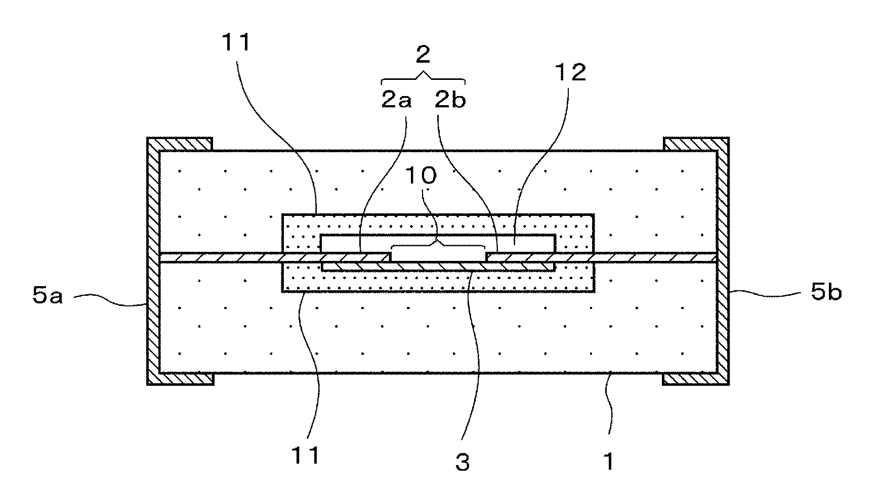
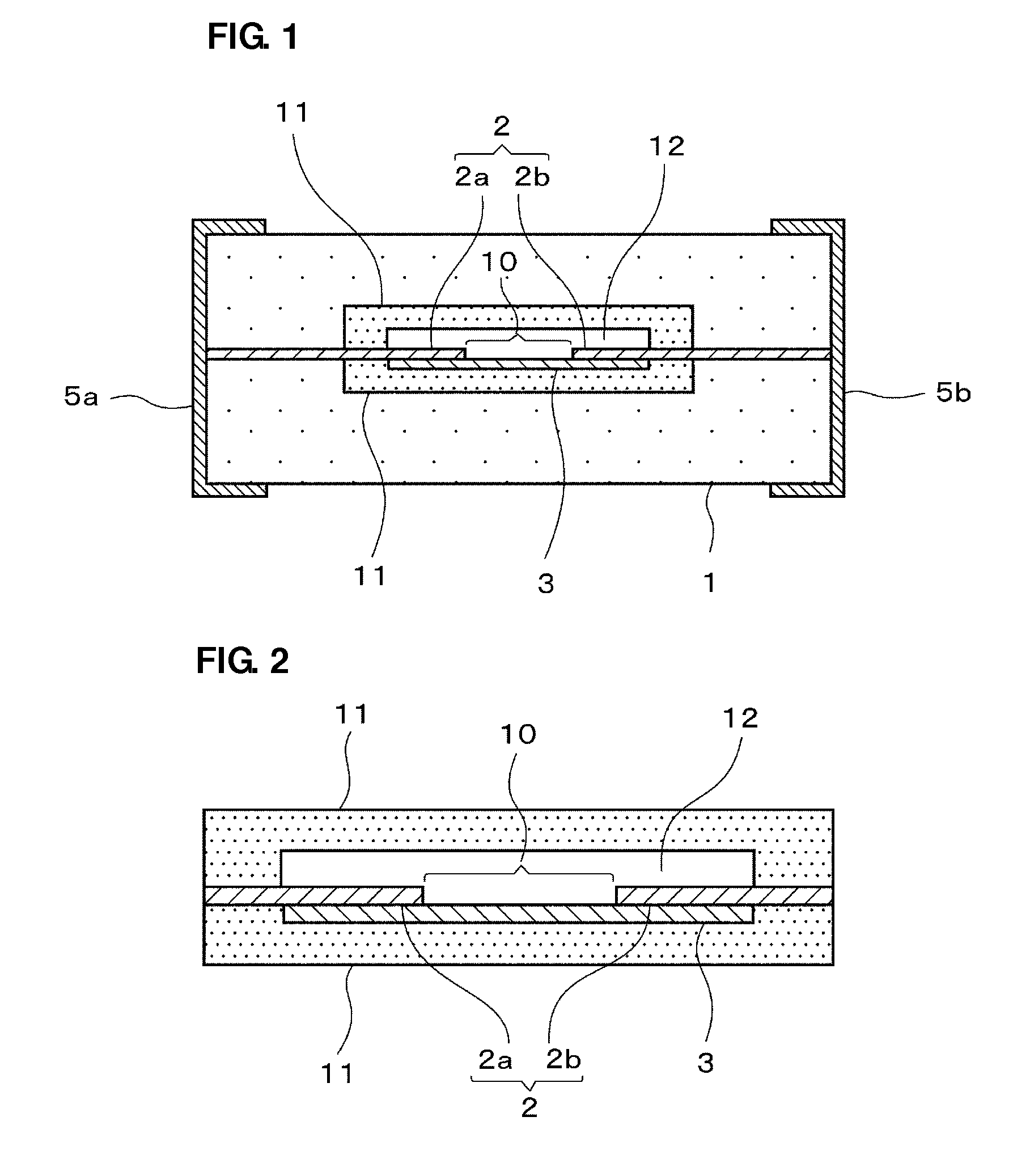
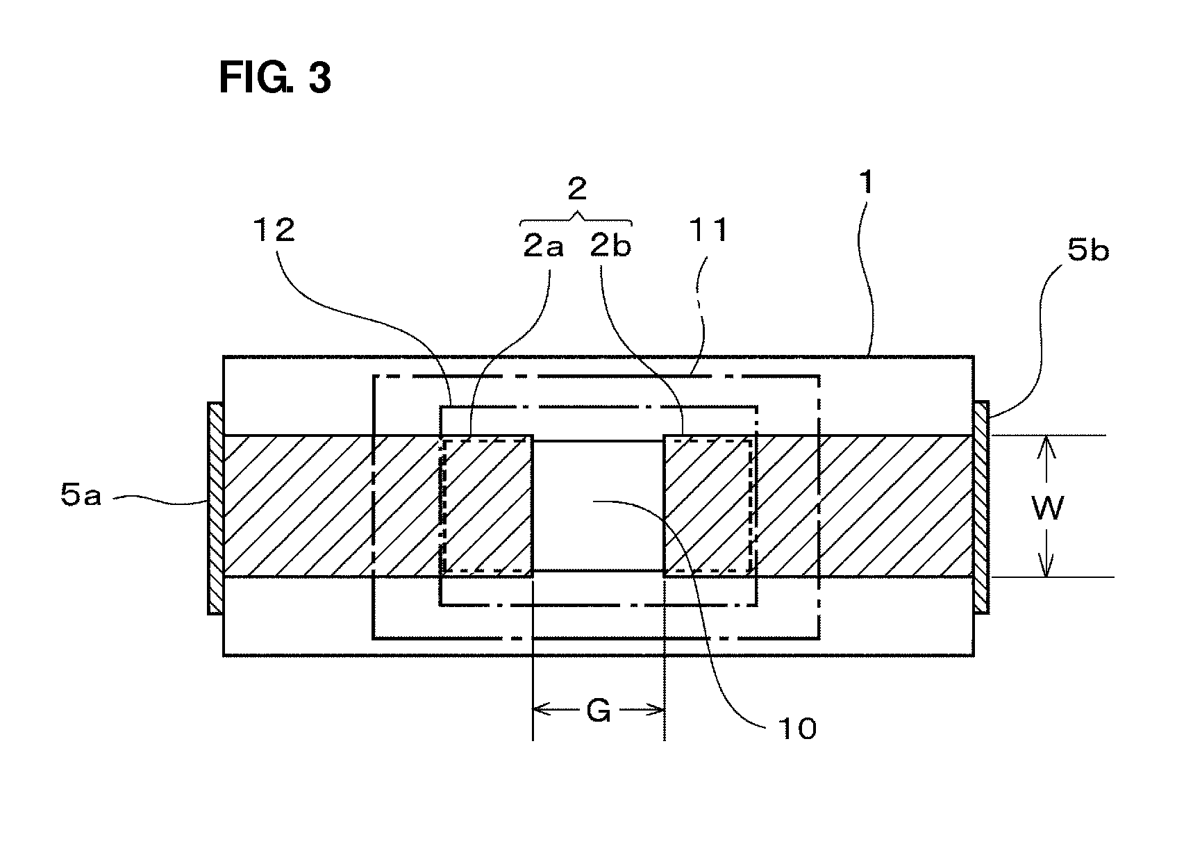
[0032]FIG. 1 is a cross-sectional view schematically illustrating the structure of an ESD protection device according to a preferred embodiment of the present invention, FIG. 2 is an enlarged front cross-sectional view illustrating an enlarged main section of the ESD protection device, and FIG. 3 is a plan cross-sectional view of the ESD protection device according to a preferred embodiment of the present invention.

[0033]This ESD protection device includes, as shown in FIGS. 1 to 3, a ceramic base material 1, opposed electrodes (extraction electrodes) 2 including an opposed electrode 2a on one side and an opposed electrode 2b on the other side, which are located in the same plane in the ceramic base material 1, and include ends opposed to each other, a discharge auxiliary electrode 3 in partial contact with the opposed electrode 2a on one s...


PUM

PropertyMeasurementUnit
thicknessaaaaaaaaaa
particle diameteraaaaaaaaaa
average particle diameteraaaaaaaaaa

Abstract

An ESD protection device includes opposed electrodes in a ceramic base material and a discharge auxiliary electrode in contact with each of the opposed electrodes which is arranged so as to provide a bridge from the opposed electrode on one side to the opposed electrode on the other side, the discharge auxiliary electrode includes metallic particles, semiconductor particles, and a vitreous material, and bonding is provided through the vitreous material between the metallic particles, between the semiconductor particles, and between the metallic particles and the semiconductor particles. The metallic particles have an average particle diameter X of about 1.0 μm or more, and the relationship between the thickness Y of the discharge auxiliary electrode and the average particle diameter X of the metallic particles satisfies about 0.5≦Y / X≦ about 3.

Description

BACKGROUND OF THE INVENTION[0001]1. Field of the Invention[0002]The present invention relates to an ESD protection device to protect a semiconductor device, etc. from electrostatic discharge (ESD) failures, and a method for manufacturing such an ESD protection device.[0003]2. Description of the Related Art[0004]In recent years, for the use of commercial-off-the-shelf appliances, there has been a tendency to increase the frequency of inserting and removing cables as input-output interfaces, and consequently, static electricity is likely to be applied to input-output connector areas. In addition, miniaturization in design with an increase in signal frequency has made it difficult to create paths, and LSI itself has been highly sensitive to static electricity.[0005]Therefore, ESD protection devices have been used widely for protecting semiconductor devices such as LSI from electrostatic discharge (ESD).[0006]As this type of ESD protection device, an overvoltage protection element has b...

Claims


Application Information

Patent Timeline
Patent Type & Authority Patents(United States)
IPC IPC(8): H01C7/10
CPCH01C7/108H01C7/12H01L23/60H01L27/0288H01T1/20H01T4/12H01T21/00H01L2924/09701H01L2924/12044H01L2924/0002H01L2924/00H01T4/10
Inventor HIEHATA, KUMIKOSUMI, TAKAHIROADACHI, JUNURAKAWA, JUNTSUKIZAWA, TAKAYUKI
Owner MURATA MFG CO LTD
Why Eureka
Try Eureka