
Structural migration of integrated circuit layout

a technology of integrated circuits and layouts, applied in the field of structural migration of integrated circuit layouts, can solve the problems of imposing a high burden on designers, time-consuming and resource-consuming custom design,

Inactive Publication Date: 2013-04-16
GLOBALFOUNDRIES INC
View PDF17 Cites 9 Cited by
  • Summary
  • Abstract
  • Description
  • Claims
  • Application Information

AI Technical Summary

Benefits of technology

This approach enables efficient and automated migration of integrated circuit layouts, reducing design burdens by allowing for quick adaptation to new technologies, improving design productivity, and maintaining structural and functional relationships, thus addressing the limitations of traditional methods.

Problems solved by technology

However, custom design is very time-consuming and resource-consuming.
When migrating from one fabrication technology to a newer, more efficient technology, array macros must often be completely redesigned to accommodate the requirements and allowances of the new technology, imposing a high burden on designers.

Method used


Image

  • Structural migration of integrated circuit layout
  • Structural migration of integrated circuit layout
  • Structural migration of integrated circuit layout

Examples


Embodiment Construction

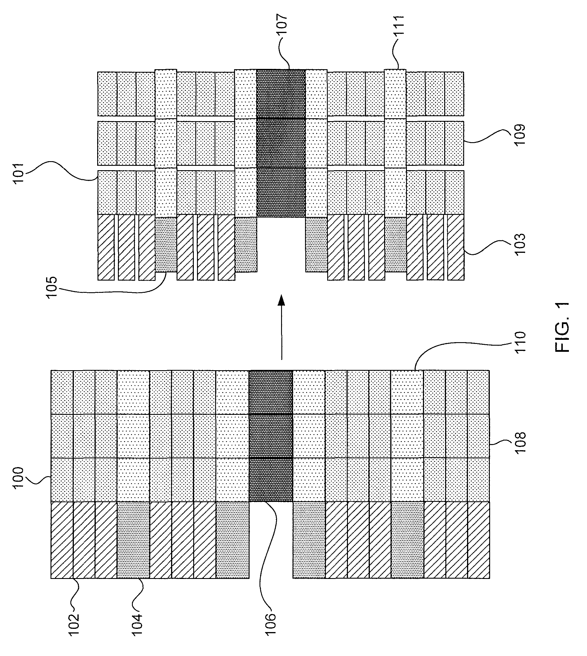
[0021]As fabrication techniques develop and change, integrated circuit (IC) layouts are adapted to take advantage of new technologies. Such a new technology may include a new fabrication process that allows etching at a smaller scale across the entire layout, or the technology may include an improved design for a particular component that allows for a reduction in size, while other components remain the same or are reduced but to a lesser degree. As a result of migrating a layout to such a technology, differing units and macros in a hierarchical layout may scale by different amounts. Such differential scaling poses a challenge for automating the migration process.

[0022]Automatic IC layout migration according to the present principles may be employed to quickly modify a layout from one technology to another technology in order to improve design productivity. The present principles may also be employed for circuit performance tuning and design for manufacturing. For example, a symboli...


PUM


Abstract

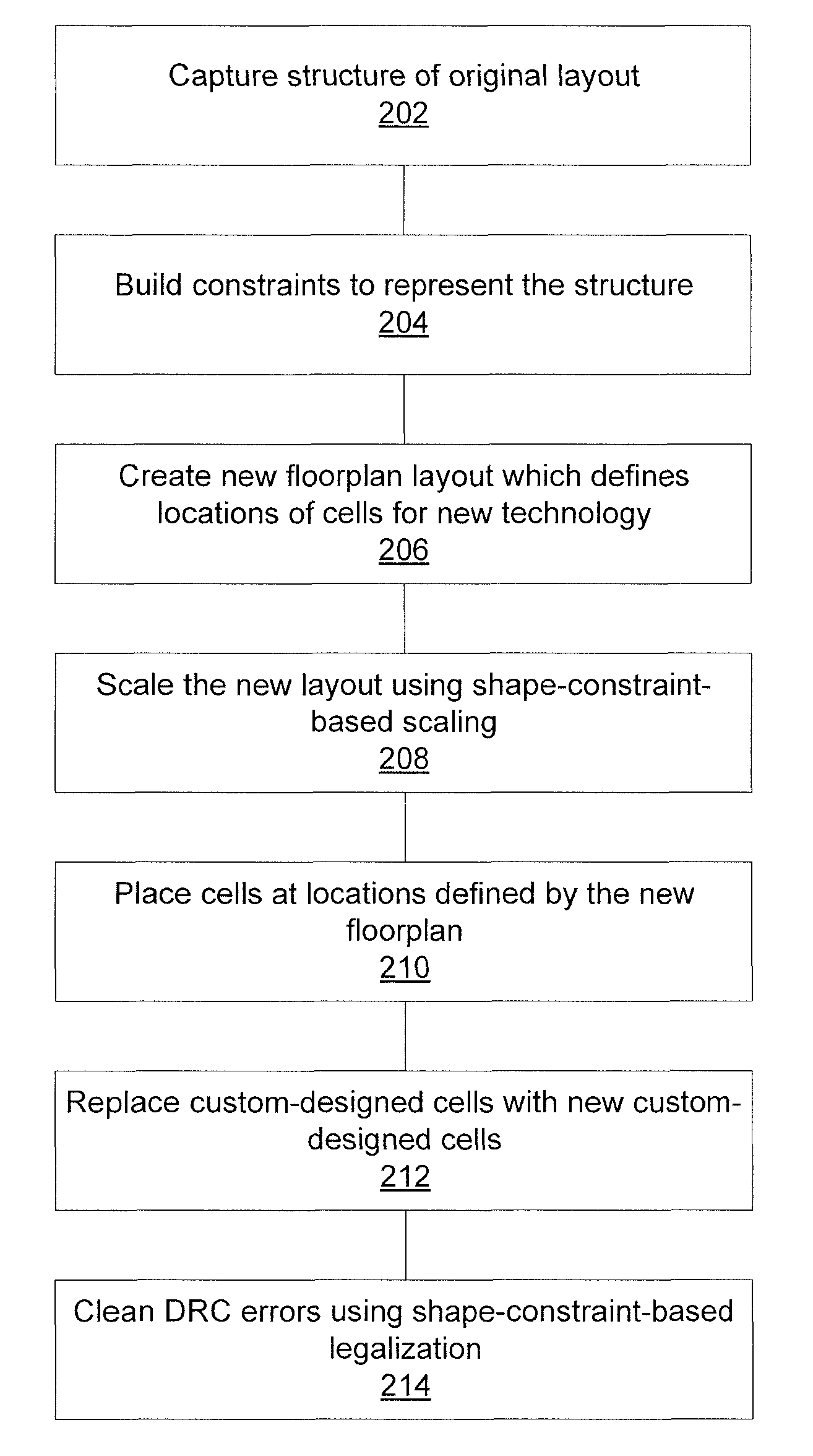
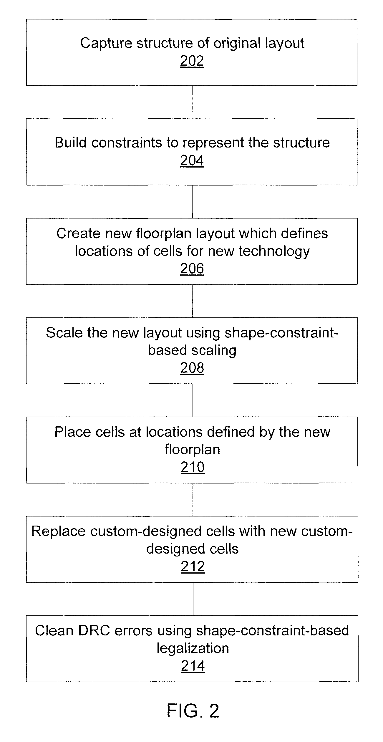
Methods and systems for migrating circuit layouts. A floorplan layout is built for a target circuit using a subset of constraints that characterize a layout structure of an original circuit. Shape-constraint-based scaling is used on the floorplan layout by scaling parts of the floorplan layout in accordance with a plurality of different scaling ratios such that portions of the floorplan layout are concurrently scaled with the plurality of different scaling ratios. Cells are placed at locations defined by the floorplan layout. The floorplan layout is checked with shape-constraint-based legalization using all of the constraints to produce a migrated layout.

Description

BACKGROUND[0001]1. Technical Field[0002]The present invention relates to integrated circuit migration and, more particularly, to methods and systems for migrating an integrated circuit layout from a first fabrication technology to a second fabrication technology.[0003]2. Description of the Related Art[0004]Integrated circuit (IC) layout is usually designed and organized hierarchically. The hierarchical representation of IC layout not only carries the designers' intent and enables a “divide-and-conquer” design principle, but also makes design checking and verification easier. Typically, a modern microprocessor includes a number of separate functional units. Each unit further includes a number of macros. A macro itself may again include a number of levels of design hierarchy with different orientations of cell placement. Array macros (such as static random access memory (SRAM) arrays) belong to a special kind of macros, which are highly structural. For example, an SRAM array contains ...

Claims


Application Information

Patent Timeline
Patent Type & Authority Patents(United States)
IPC IPC(8): G06F17/50
CPCG06F17/5068G06F30/39
Inventor HENG, FOOK-LUENJOSHI, RAJIV V.LVOV, ALEXEY Y.TANG, XIAOPING
Owner GLOBALFOUNDRIES INC
Learn More