

Apparatus for thermally treating semiconductor substrates
- Summary
- Abstract
- Description
- Claims
- Application Information
AI Technical Summary
Benefits of technology
Problems solved by technology
Method used
Image

Examples
Embodiment Construction
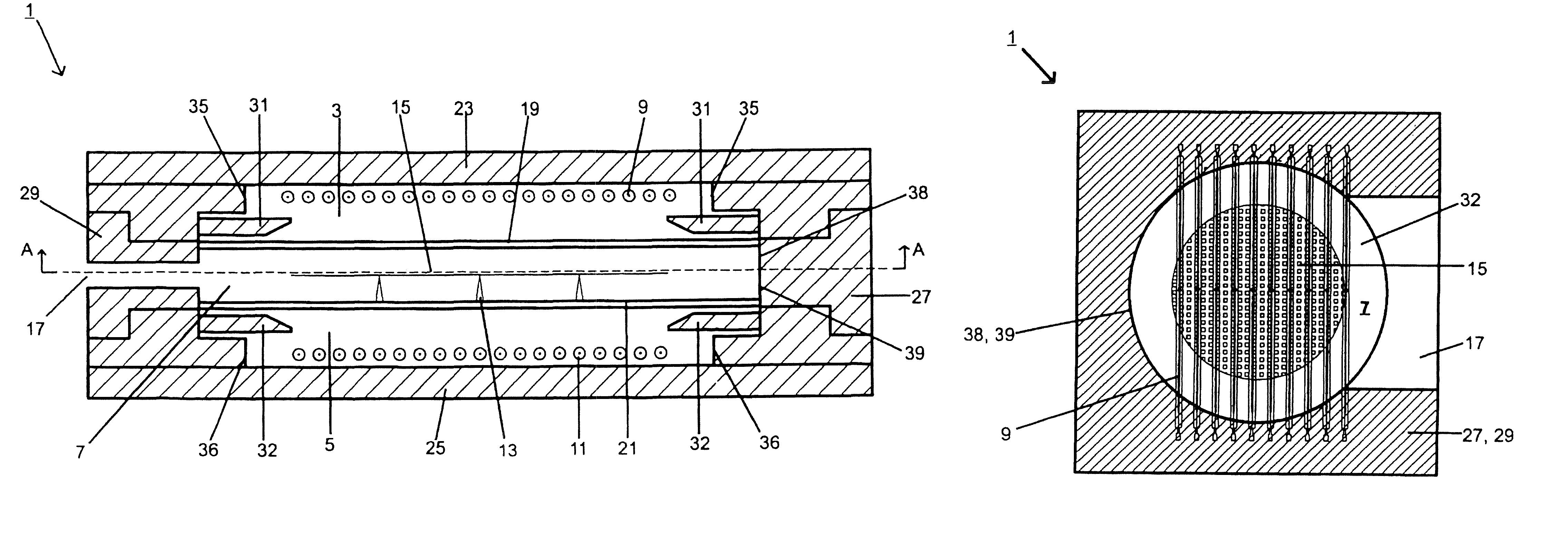
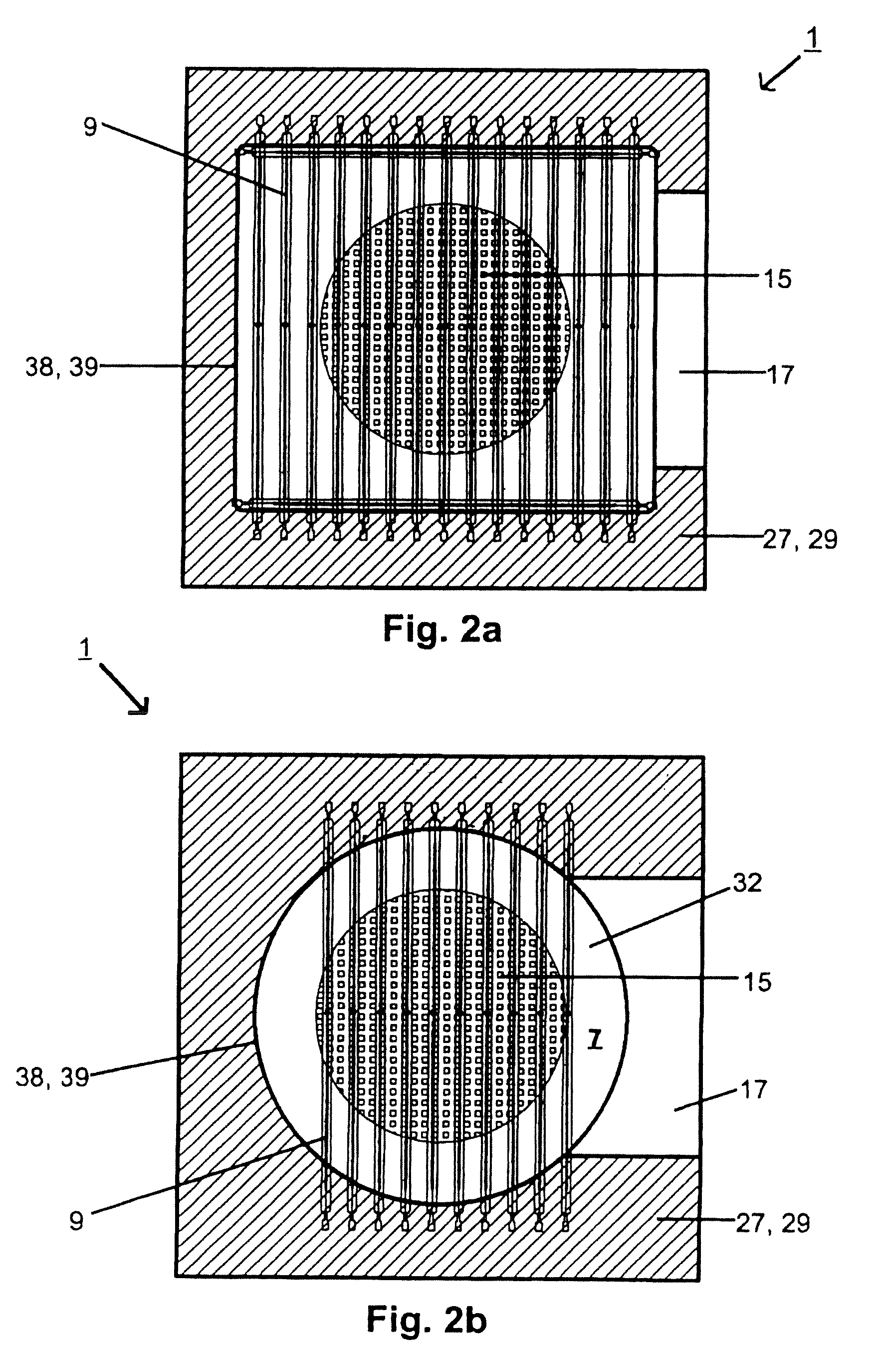
[0035]FIG. 1 shows a cross-section of a processing chamber 1 of a rapid heating system for thermally treating semiconductor wafers. Located within the processing chamber 1 is the processing space 3, 5, 7 comprising an upper lamp chamber 3, a lower lamp chamber 5 and a reaction chamber 7. The upper and the lower lamp chambers each have a row of heating elements 9, 11, which are preferably rod-shaped, but can also be in the form of spot lights or surface radiation elements. The heating elements are preferably halogen lamps and / or arc lamps.
[0036]The reaction chamber 7 has a substrate holding device 13 which defines a substrate retaining region 15 for receiving a disc-shaped semiconductor substrate, such as for example a silicon wafer, which may be inserted through a door opening 17. Gas inlets and gas outlets (not shown) may be disposed in the reaction chamber by means of which a process gas can be conveyed to the semiconductor substrate. The upper and the lower lamp chambers can be s...
PUM
 Abstract
Description
Claims
Application Information