Capping layer for reduced outgassing

a technology of capping layer and outgassing, which is applied in the direction of coating, chemical vapor deposition coating, metallic material coating process, etc., can solve the problems of prone to dielectric material depositing, structural features of the device having decreased spatial dimensions, and difficulty in filling the gap with dielectric material

Inactive Publication Date: 2013-06-18
APPLIED MATERIALS INC
View PDF430 Cites 138 Cited by
  • Summary
  • Abstract
  • Description
  • Claims
  • Application Information

AI Technical Summary

Problems solved by technology

The decreasing feature sizes result in structural features on the device having decreased spatial dimensions.
The widths of gaps and trenches on the device narrow to a point where the aspect ratio of gap depth to its width becomes high enough to make it challenging to fill the gap with dielectric material.
The depositing dielectric material is prone to clog at the top before the gap completely fills, producing a void or seam, in the middle of the gap.
However, once these highly flowable materials are deposited, they have to be hardened into a solid dielectric material.
Unfortunately, the departing carbon and hydroxyl species often leave behind pores in the hardened dielectric that reduce the quality of the final material.
In addition, the hardening dielectric also tends to shrink in volume, which can leave cracks and spaces at the interface of the dielectric and the surrounding substrate.
Thermal budget considerations have largely limited SOD to process flows incorporating an underlying silicon nitride layer which can protect underlying features from oxidation (e.g. DRAM applications).

Method used


Image

  • Capping layer for reduced outgassing
  • Capping layer for reduced outgassing
  • Capping layer for reduced outgassing

Examples


Embodiment Construction

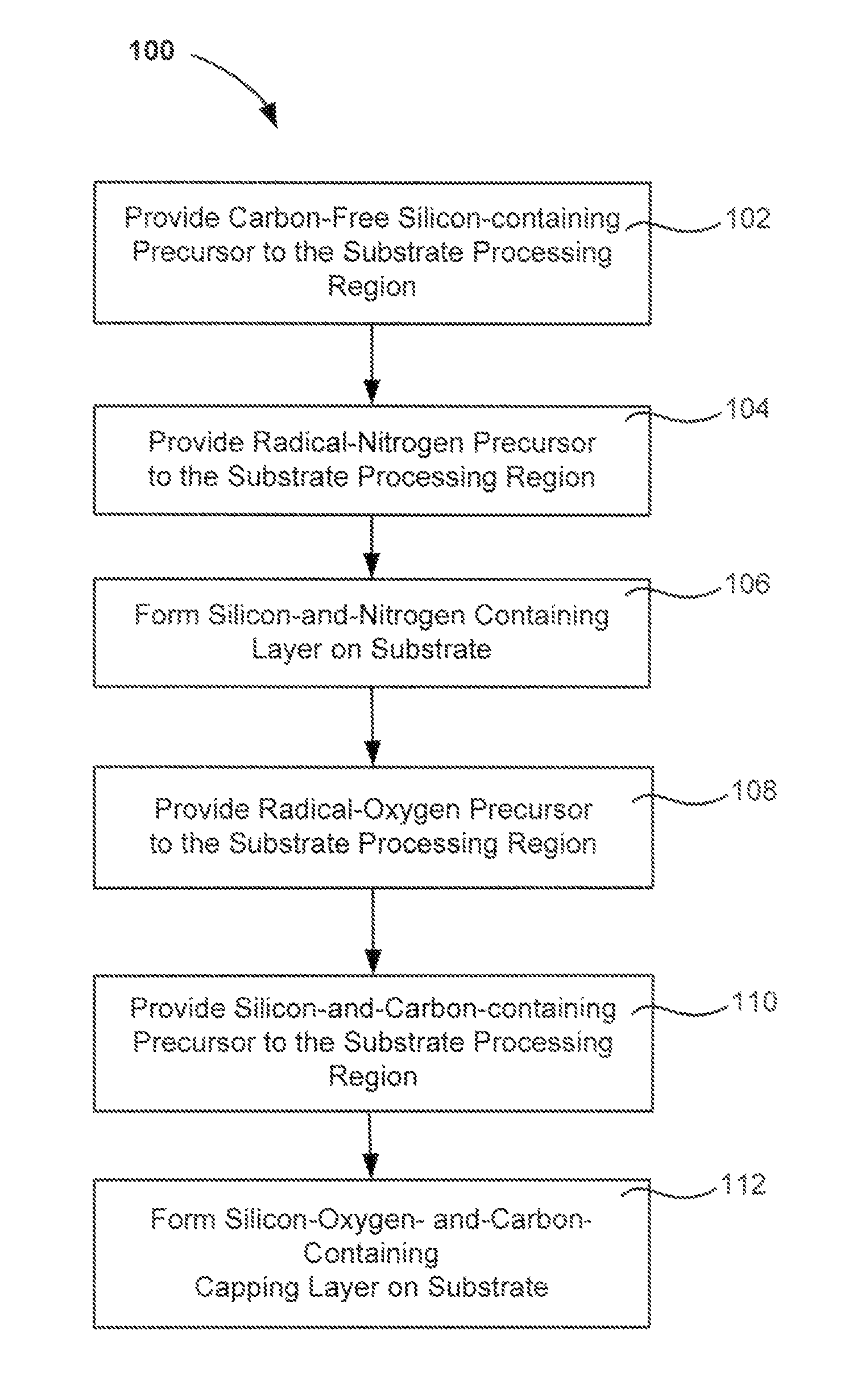
[0015]A method of forming a silicon oxide layer is described. The method first deposits a silicon-nitrogen-and-hydrogen-containing (polysilazane) film by radical-component chemical vapor deposition (CVD). The silicon-nitrogen-and-hydrogen-containing film is formed by combining a radical precursor (excited in a remote plasma) with an unexcited carbon-free silicon precursor. A capping layer is formed over the silicon-nitrogen-and-hydrogen-containing film to avoid time-evolution of underlying film properties prior to conversion into silicon oxide. The capping layer is formed by combining a radical oxygen precursor (excited in a remote plasma) with an unexcited silicon-and-carbon-containing-precursor. The films are converted to silicon oxide by exposure to oxygen-containing environments. The two films may be deposited within the same substrate processing chamber and may be deposited without breaking vacuum.

[0016]Capping a radical-component CVD silicon-nitrogen-and-hydrogen-containing fi...


PUM

PropertyMeasurementUnit
temperatureaaaaaaaaaa

Abstract

A method of forming a silicon oxide layer is described. The method first deposits a silicon-nitrogen-and-hydrogen-containing (polysilazane) film by radical-component chemical vapor deposition (CVD). The silicon-nitrogen-and-hydrogen-containing film is formed by combining a radical precursor (excited in a remote plasma) with an unexcited carbon-free silicon precursor. A capping layer is formed over the silicon-nitrogen-and-hydrogen-containing film to avoid time-evolution of underlying film properties prior to conversion into silicon oxide. The capping layer is formed by combining a radical oxygen precursor (excited in a remote plasma) with an unexcited silicon-and-carbon-containing-precursor. The films are converted to silicon oxide by exposure to oxygen-containing environments. The two films may be deposited within the same substrate processing chamber and may be deposited without breaking vacuum.

Description

CROSS-REFERENCES TO RELATED APPLICATIONS[0001]This application claims the benefit of U.S. Provisional Application No. 61 / 492,914 by Wang et al, filed Jun. 3, 2011 and titled “CAPPING LAYER FOR REDUCED OUTCLASSING” which is incorporated herein in its entirety for all purposes.BACKGROUND OF THE INVENTION[0002]Semiconductor device geometries have dramatically decreased in size since their introduction several decades ago. Modern semiconductor fabrication equipment routinely produce devices with 45 nm, 32 nm, and 28 nm feature sizes, and new equipment is being developed and implemented, to make devices with even smaller geometries. The decreasing feature sizes result in structural features on the device having decreased spatial dimensions. The widths of gaps and trenches on the device narrow to a point where the aspect ratio of gap depth to its width becomes high enough to make it challenging to fill the gap with dielectric material. The depositing dielectric material is prone to clog a...

Claims


Application Information

Patent Timeline
Patent Type & Authority Patents(United States)
IPC IPC(8): H01L21/316
CPCC23C16/30C23C16/452C23C16/56H01L21/02164H01L21/022H01L21/02211H01L21/02219H01L21/02323H01L21/02326
Inventor WANG, LINLINMALLICK, ABHIJIT BASUINGLE, NITIN K.
Owner APPLIED MATERIALS INC
Why Eureka
Try Eureka