Surface-PlasmonoDielectric-polaritonic devices and systems

a surface-plasmonodielectric-polaritonic and device technology, applied in the direction of optical waveguide light guide, light demodulation, instruments, etc., can solve the problems of system bandwidth delay product, non-ideal wavepacket propagation, and limit the achievable, so as to achieve superior system performance and extend the effect of capabilities

Inactive Publication Date: 2013-06-25
MASSACHUSETTS INST OF TECH
View PDF8 Cites 5 Cited by
  • Summary
  • Abstract
  • Description
  • Claims
  • Application Information

AI Technical Summary

Problems solved by technology

One fundamental challenge for such modern photonic systems is the desire, for many applications, to operate as a substantially perfect light-guiding system by supporting, over a large frequency bandwidth, subwavelength modes of small group velocity and small attenuation, both substantially devoid of frequency dispersion.
But conventional photonic systems exhibit modal dispersion that disallows such performance and that results in, e.g., limitation of the achievable so-called ‘bandwidth-delay product’ of the system, whereby only non-ideal wavepacket propagation is achievable.
But such configurations are limited in their applicability to general photonic device arrangements and photonic applications, including SPP-based devices and applications.

Method used


Image

  • Surface-PlasmonoDielectric-polaritonic devices and systems
  • Surface-PlasmonoDielectric-polaritonic devices and systems
  • Surface-PlasmonoDielectric-polaritonic devices and systems

Examples


example i

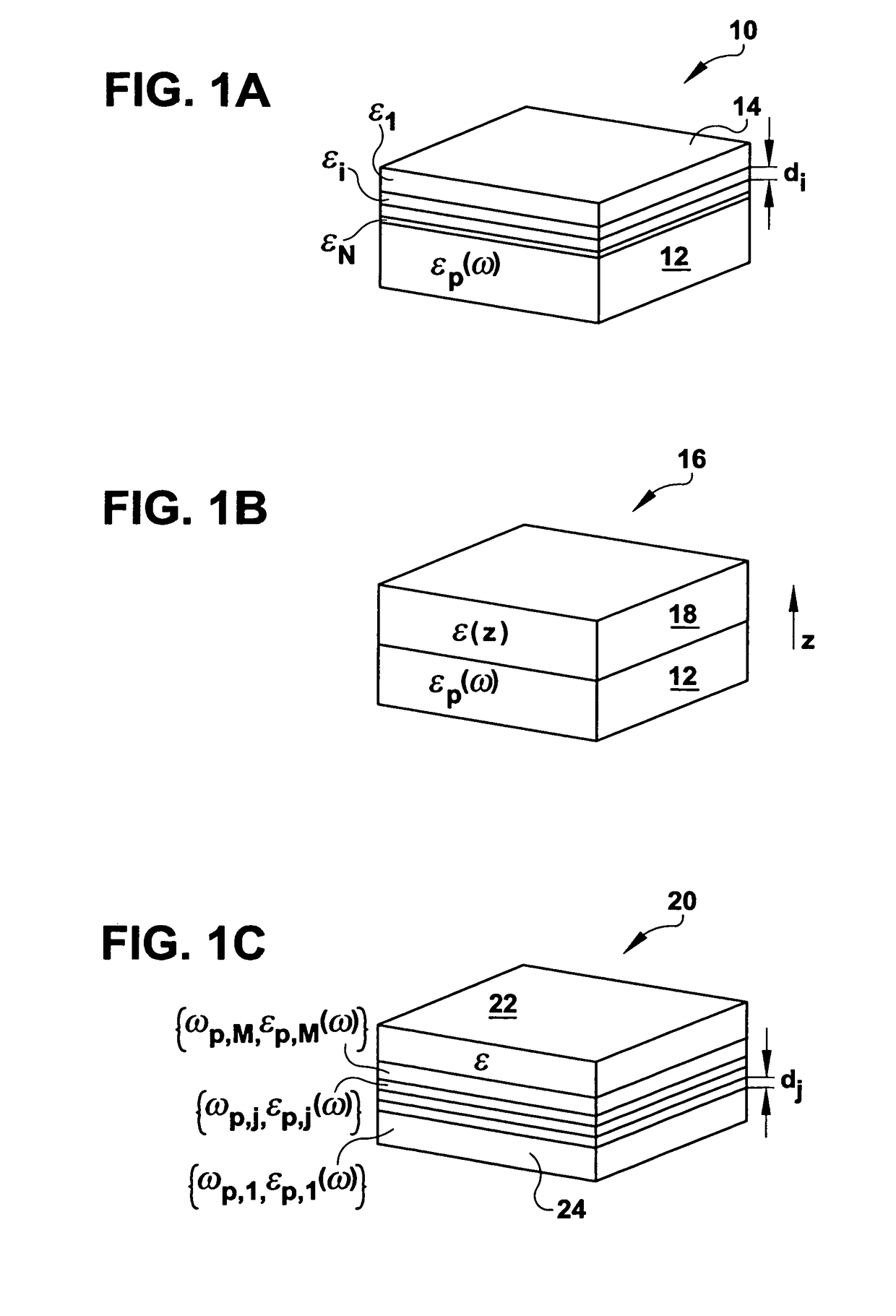
[0112]An SPDP structure having a layered dielectric region adjacent to a homogeneous plasmonic material region, as in FIG. 1A, was designed. The dispersion relation engineering method described above was employed to determine a dispersion relation for the SPDP structure so that the diagram of the frequency-wavevector correspondence specifically resembled the letters “MIT.”FIG. 5A is a plot of this diagram of frequency as a function of wavevector, here both normalized to the plasmonic values.

[0113]To achieve this dispersion relation, the SPDP structure was defined with the permittivity surrounding the structure set as ε=1 and the plasmonic high-frequency permittivity set as ε∞=1. It was found that nine dielectric layers were required to achieve this dispersion relation. From the top to the bottom of the stack of nine dielectric layers, the permittivities were given as εi={4, 1, 10, 1, 10, 1.7, 1, 10, 1.7}. The thicknesses of the nine dielectric layers, from the top to the bottom of t...

example ii

[0115]An SPDP structure having a layered dielectric region adjacent to a homogeneous plasmonic material region, as in FIG. 1A, was designed as in Example I, and the dispersion relation engineering method described above was employed to determine a dispersion relation for the SPDP structure so that dispersion would be substantially suppressed to a high-order. The dispersion relation was further specified for a positive group velocity. FIG. 6A illustrates the resulting dispersion diagram, plotted as frequency as a function of wavevector, here both normalized to the plasmonic values.

[0116]To achieve this dispersion relation, the SPDP structure was defined with the permittivity surrounding the structure set as ε=1 and the plasmonic high-frequency permittivity set as ε∞=1. It was found that four dielectric layers were required to achieve this dispersion relation. From the top to the bottom of the stack of four dielectric layers, the permittivities were given as εi={4, 1, 4, 1}. The thick...

example iii

[0119]An SPDP structure having a layered dielectric region adjacent to a homogeneous plasmonic material region, as in FIG. 1A, was designed as in Example I, and the dispersion relation engineering method described above was employed to determine a dispersion relation for the SPDP structure so that dispersion would be substantially suppressed to a high-order. The dispersion relation was further specified for a negative group velocity. FIG. 7A illustrates the resulting dispersion diagram, plotted as frequency as a function of wavevector, here both normalized to the plasmonic values.

[0120]To achieve this dispersion relation, the SPDP structure was defined with the permittivity surrounding the structure set as ε=1 and the plasmonic high-frequency permittivity set as ε∞=1. It was found that five dielectric layers were required to achieve this dispersion relation. From the top to the bottom of the stack of five dielectric layers, the permittivities were given as εi={4, 1, 4, 1, 4}. The th...


PUM

PropertyMeasurementUnit
surface plasmon polaritonsaaaaaaaaaa
dielectric permittivityaaaaaaaaaa
metallicaaaaaaaaaa

Abstract

There is provided a structure for supporting propagation of surface plasmon polaritons. The structure includes a plasmonic material region and a dielectric material region, disposed adjacent to a selected surface of the plasmonic material region. At least one of the plasmonic material region and the dielectric material region have a dielectric permittivity distribution that is specified as a function of depth through the corresponding material region. This dielectric permittivity distribution is selected to impose prespecified group velocities, vgj, on a dispersion relation for a surface polaritonic mode of the structure for at least one of a corresponding set of prespecified frequencies, ωj, and corresponding set of prespecified wavevectors, where j=1 to N.

Description

CROSS-REFERENCE TO RELATED APPLICATIONS[0001]This application claims the benefit of U.S. Provisional Application No. 61 / 123,603, filed Apr. 10, 2008, the entirety of which is hereby incorporated by reference.STATEMENT REGARDING FEDERALLY SPONSORED RESEARCH[0002]This invention was made with Government support under Grant No. DMR0819762 awarded by the National Science Foundation, Grant No. DE-FG02-99ER45778 awarded by the Department of Energy, and Grant No. W911NF-07-D-0004 awarded by the Army. The Government has certain rights in the invention.BACKGROUND OF THE INVENTION[0003]This invention relates to photonic technology for guiding surface-plasmon-polaritons, and more particularly relates to control of dispersion in surface-plasmon-polariton propagation.[0004]There is increasing interest in the design of surface-plasmon-polariton (SPP) photonic and optoelectronic systems; the unique light guiding properties of such SPP-based systems, such as subwavelength guiding of nanoscaled light...

Claims


Application Information

Patent Timeline
Patent Type & Authority Patents(United States)
IPC IPC(8): G02B6/10
CPCB82Y20/00G02B6/1226G02F1/365G02F2203/10
Inventor KARALIS, ARISTEIDISJOANNOPOULOS, JOHNSOLJACIC, MARIN
Owner MASSACHUSETTS INST OF TECH
Why Eureka
Try Eureka