Apparatus for the detection of light in a scanning microscope

a scanning microscope and apparatus technology, applied in the field of light detectors, can solve the problems of saturation limit the maximum obtainable signal per pixel, insufficient fluorescence photons, signal-to-noise ratio and/or signal strength of signals to be detected, etc., and achieve the effect of quick and reliable acquisition of image data

Active Publication Date: 2013-08-06
LEICA MICROSYSTEMS CMS GMBH
View PDF16 Cites 2 Cited by
  • Summary
  • Abstract
  • Description
  • Claims
  • Application Information

AI Technical Summary

Benefits of technology

[0014]It is therefore an object of the present invention to provide a light detector which is particularly suited for use in scanning microscopes and which avoids the problems of known arrangements described above. In particular the light detector is to enable a quick and reliable acquisition of image data.
[0022]The line array provides a substantial advantage for use in scanning microscopy when compared to point scanners in that the time available for the detection of photons is multiplied by the number of pixels of a line array. An entire line of an image can be read out with high sensitivity and considerably reduced noise as compared to usual CCD arrays. It is also possible to detect single photons. Moreover the trigger circuit can be implemented such that as opposed to common CCD arrays all picture elements, i.e. all avalanche semiconductor diodes, can be read out at the same time. This results in a considerably increased detection speed.
[0029]This modification of the invention provides the advantage that the active area of a picture element on an image line is now doubled and at the same time divided into two subareas (or more, depending on the number of line arrays) which can be read out independently. It is highly likely that during the dead time of one avalanche semiconductor detector the second avalanche semiconductor detector is active, so that this second detector can continue to register photons. In this way the problem caused by dead times of avalanche semiconductor detectors is greatly reduced.
[0032]For any one of the above described accumulating or counting processes the parallel counter may in particular comprise a memory area including several memory cells. These memory cells can then be assigned to single avalanche semiconductor detectors of the line arrays or of one line array. Preset values (for example the preset value “1”) may be assigned to these memory cells, which preset values correspond to an idle state in which no signals are detected. The trigger circuit may then be configured to temporarily increase or lower the value of the memory cell whenever one or more of the avalanche semiconductor detectors assigned to this memory cell detect a light pulse. In case a single photon is detected, for instance, the value of the memory cell assigned to the avalanche semiconductor detector which has detected the photon can be lowered temporarily from the value “1” to the value “0”. The string of values of the memory cells which can be read out may then for example correspond to the image information of the line detector. Also accumulation can be easily carried out this way, for instance by accumulating those bit strings of the line array which have been registered during the counting time in a corresponding manner. Also the accumulation of a plurality of line arrays, for instance of two line arrays arranged in parallel, or the accumulation of the avalanche semiconductor detectors assigned to the same picture element on one line, respectively, can be easily realized in this manner. The values of the memory cell can be reset to the original preset values after the detection has taken place and / or with a preset reading-out clock rate so that the counting can start anew.
[0038]This is due to the fact that a coherent signal of the sample area interferes in the pupil plane of the spatial beam splitter in such a manner that it generates the same structure in this plane as did the illumination signal irradiated before. An incoherent signal, on the other hand, is comprised of a plurality of independent point emitters, each single one of which irradiates the entire pupil plane of the spatial separation beam splitter. The sum of all point emitters thus also irradiates the entire pupil plane. This effect is used for separating the detection light coming from the sample into a coherent and a non-coherent part. The separation can be implemented with high efficiency and a high suppression ratio as well as at low cost.
[0040]The light detector described above comprising at least one line array and containing a plurality of avalanche semiconductor detectors can also be advantageously adapted in a scanning microscope such that different spectral wave length ranges of a single area of the sample can be imaged onto different avalanche semiconductor detectors of the line array or of the light detector, respectively. This is particularly advantageous when two line arrays are used. For instance a spectral separation element can be provided which separates image information of one line of the sample spectrally into at least two wave length ranges. These at least two wave length ranges may then be imaged onto different avalanche semiconductor detectors of the light detector. For instance a first wave length range may be imaged onto a first line array while a second wave length range may be imaged onto a second line array. In this case not only image information of one wave length range but image information of several wave length ranges may be acquired simultaneously at high speed, which may for instance have positive effects on the contrast or other image properties. The microscope may e.g. be adapted such that a first line array acquires image information in a spectral range containing a first peak of a fluorescent colorant of the sample, while information in a range surrounding a second peak of a fluorescent colorant of the sample may be acquired by a second line array. For spectral separation, various known spectral separation elements may be used, such as gratings and / or prisms. Also in this preferred arrangement the suggested highly sensitive light detector which can be read out quickly is particularly advantageous in that image information can be acquired simultaneously and with the highest sensitivity in different wave length ranges.

Problems solved by technology

A basic problem, which plays a major role in many of the microscopes described above as well as in other image acquisition methods, is the signal-to-noise-ratio and / or the signal strength of the signals to be detected.
In particular, in fluorescence microscopy the saturation of the colorants used becomes noticeable in this respect, which saturation limits the maximum obtainable signal per pixel.
Depending on the scanning speed and image format, often not enough fluorescence photons are available.
This arithmetic example shows that the signal-to-noise ratio is a basic problem in scanning microscopes since for procedural reasons only an extremely limited period of time is available for gathering light quantums for single pixels.
Increasing this time period however entails increasing the time for image formation which involves inconveniences for a user and / or which can lead to blurring of the image in case of quickly changing samples.
The CCD chips (charge-coupled device) normally used as image detectors in microscopes further cause additional difficulties in the form of increased noise.
For example in CCDs, in addition to shot noise, readout noise is often dominating especially at small signal levels, which noise as a rule increases even further as the speed increases.
Despite the various previous suggestions to use APD arrays in the field of microscopy, however, the use of such arrays still poses a technical challenge.
One particular difficulty consists in acquiring the great volume of data in a suitable manner and to process it at a corresponding speed.
Also in many cases the dead time, which is a known problem in APDs, leads to difficulties, since it further reduces the length of image time available for 1 pixel and increases fluctuations in the counting rates.

Method used


Image

  • Apparatus for the detection of light in a scanning microscope
  • Apparatus for the detection of light in a scanning microscope
  • Apparatus for the detection of light in a scanning microscope

Examples


first embodiment

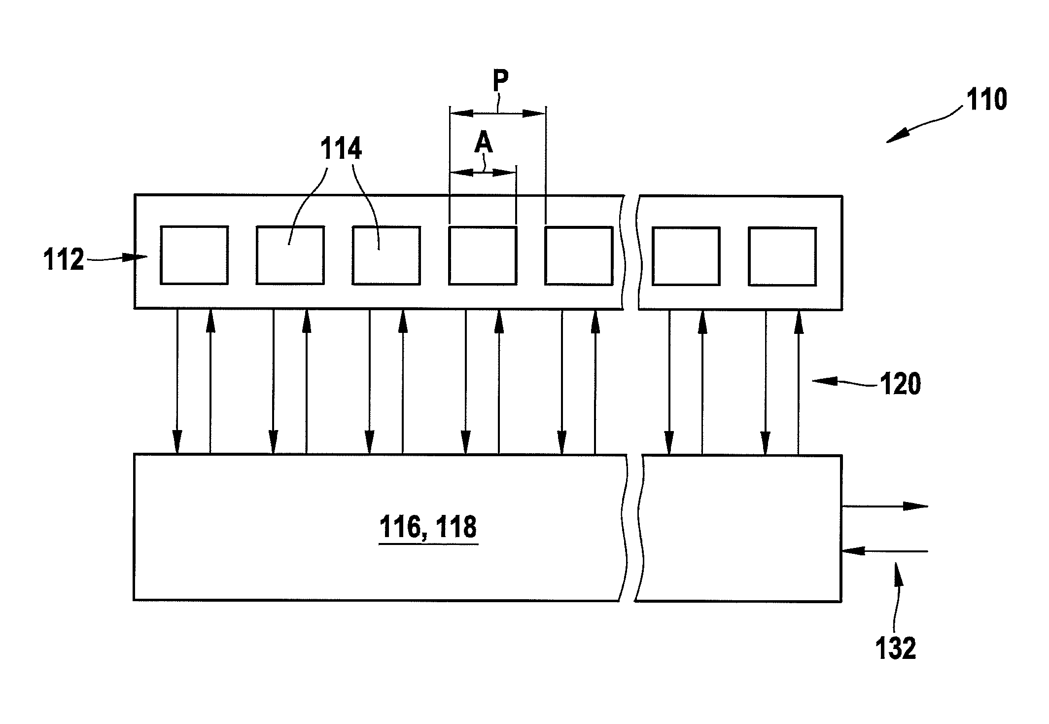
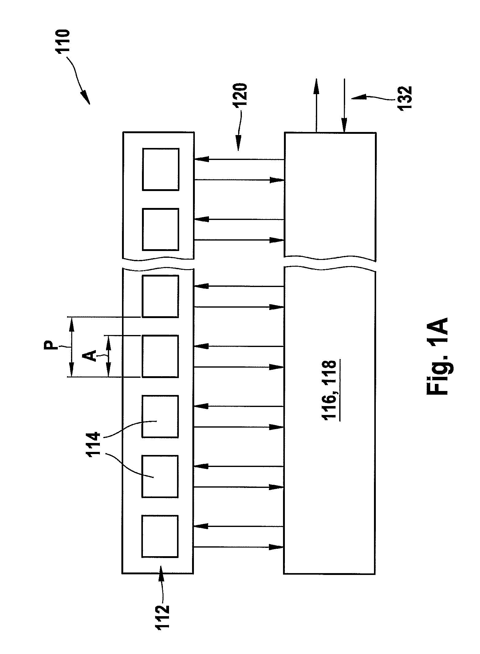
[0042]FIGS. 1A and 1B show a light detector with a line array;

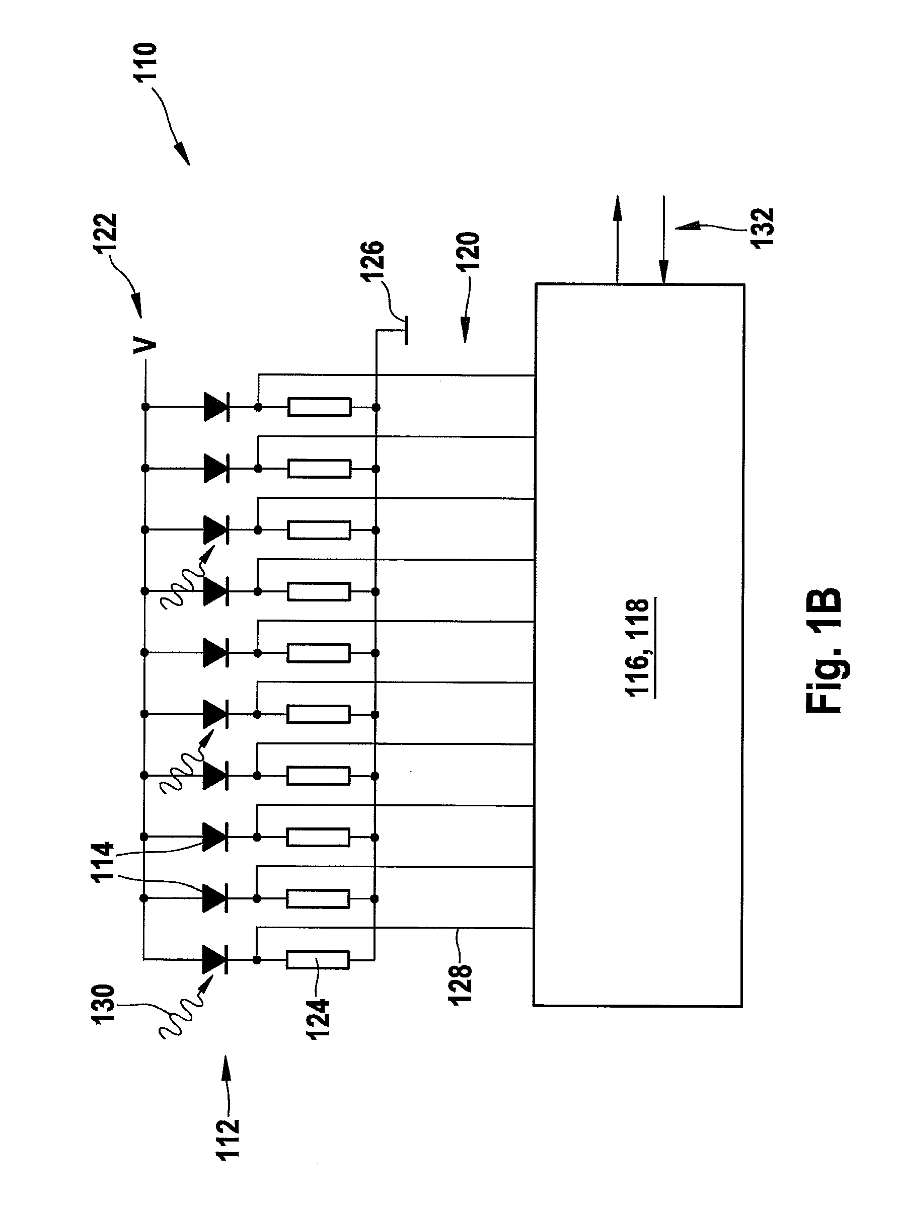
[0043]FIG. 1C shows an embodiment of an active quenching circuit for an APD of the line array according to FIGS. 1A and 1B;

second embodiment

[0044]FIGS. 2A and 2B show a light detector with two line arrays;

[0045]FIG. 3 shows a first embodiment according to the invention of a line scanning microscope comprising a spatial beam splitter and a light detector according to the invention;

[0046]FIG. 4 shows a second embodiment of a line scanning microscope comprising an additional dichroic beam splitter arranged in the detection light path; and

third embodiment

[0047]FIG. 5 shows a line scanning microscope comprising a prism arranged in the detection light path.

DETAILED DESCRIPTION OF THE DRAWINGS

[0048]FIGS. 1A and 1B depict a first embodiment of a light detector 110 according to the invention. FIG. 1A shows the external construction of the light detector 110 while FIG. 1B is used to schematically clarify the electric circuitry of the light detector 110.

[0049]The light detector 110 in the embodiment shown in FIG. 1A comprises a line array 112 which is constructed as a monolithic semiconductor element in this example and which comprises a plurality of avalanche semiconductor detectors 114 (also referred to as APDs in the following) arranged in series. The line array 112 has a pitch which is denoted by P in FIG. 1A and which is for instance 150 μm. The active part, which is implemented by the active areas of the APDs 114, is denoted by A in FIG. 1A. Consequently, the linear filling factor is NP and can for instance be at 50 percent or higher...


PUM


Abstract

A light detector for use in a line scanning microscope and a microscope comprising such a light detector are described. The light detector comprises a line array of avalanche semiconductor detectors; and an electronic trigger circuit that is adapted to operate the avalanche semiconductor detectors in at least one of a Geiger mode with internal charge amplification and in a linear mode. The trigger circuit further comprises a parallel counter that is designed to read out in parallel light pulses detected by the avalanche semiconductor detectors. The parallel counter is adapted to accumulate the light pulses detected by the avalanche semiconductor detectors over a preset counting time.

Description

CROSS-REFERENCE TO RELATED APPLICATIONS[0001]This application is a national phase entry based on the International Patent Application PCT / EP2008 / 055537 filed on May 6, 2008 that claims the priority of the German patent application DE 102007024074.2 dated May 22, 2007. The entire content of this prior German patent application is herewith incorporated by reference.BACKGROUND OF THE INVENTION[0002]The invention relates to a light detector for use in a scanning microscope, and in particular in a line scanning microscope. Further, the invention relates to a microscope comprising the light detector according to the invention.[0003]Scanning microscopes are used in very different fields of engineering and sciences. A basic principle of such scanning microscopes is that one or more microscope beams are deflected in one or more dimensions by means of a beam deflector arrangement in order to screen (scan) a sample.[0004]Various versions of scanning microscopes are known, which differ, for ins...

Claims


Application Information

Patent Timeline
Patent Type & Authority Patents(United States)
IPC IPC(8): G02B21/00
CPCG01J1/44G01J1/46G01J3/2803G02B21/0032G02B21/0096H01L31/107
Inventor BIRK, HOLGERSEYFRIED, VOLKER
Owner LEICA MICROSYSTEMS CMS GMBH
Why Eureka
Try Eureka