[0014]It is therefore an object of the present invention to provide a light
detector which is particularly suited for use in scanning microscopes and which avoids the problems of known arrangements described above. In particular the light detector is to enable a quick and reliable acquisition of image data.
[0022]The
line array provides a substantial
advantage for use in
scanning microscopy when compared to point scanners in that the time available for the detection of photons is multiplied by the number of pixels of a
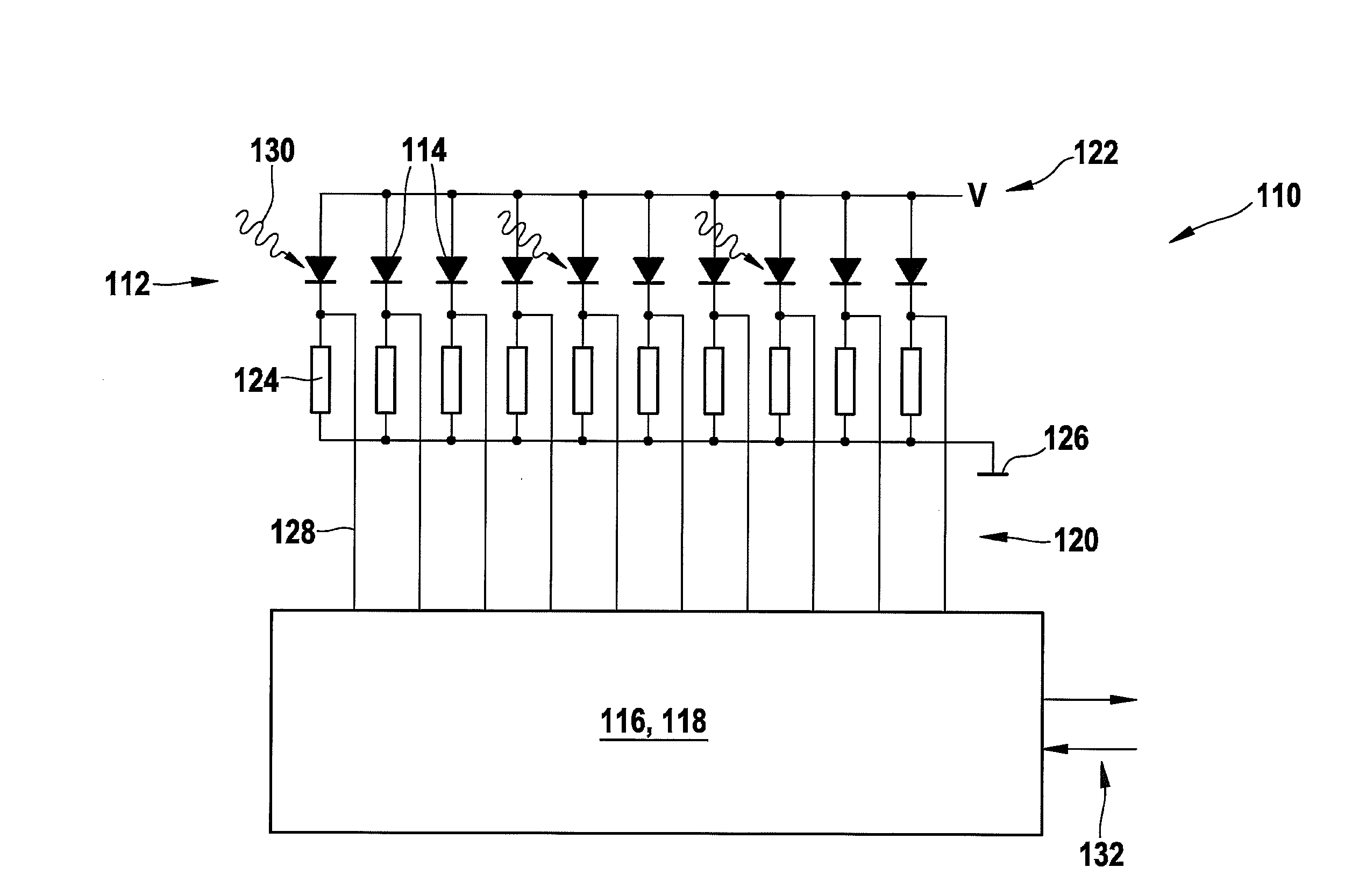
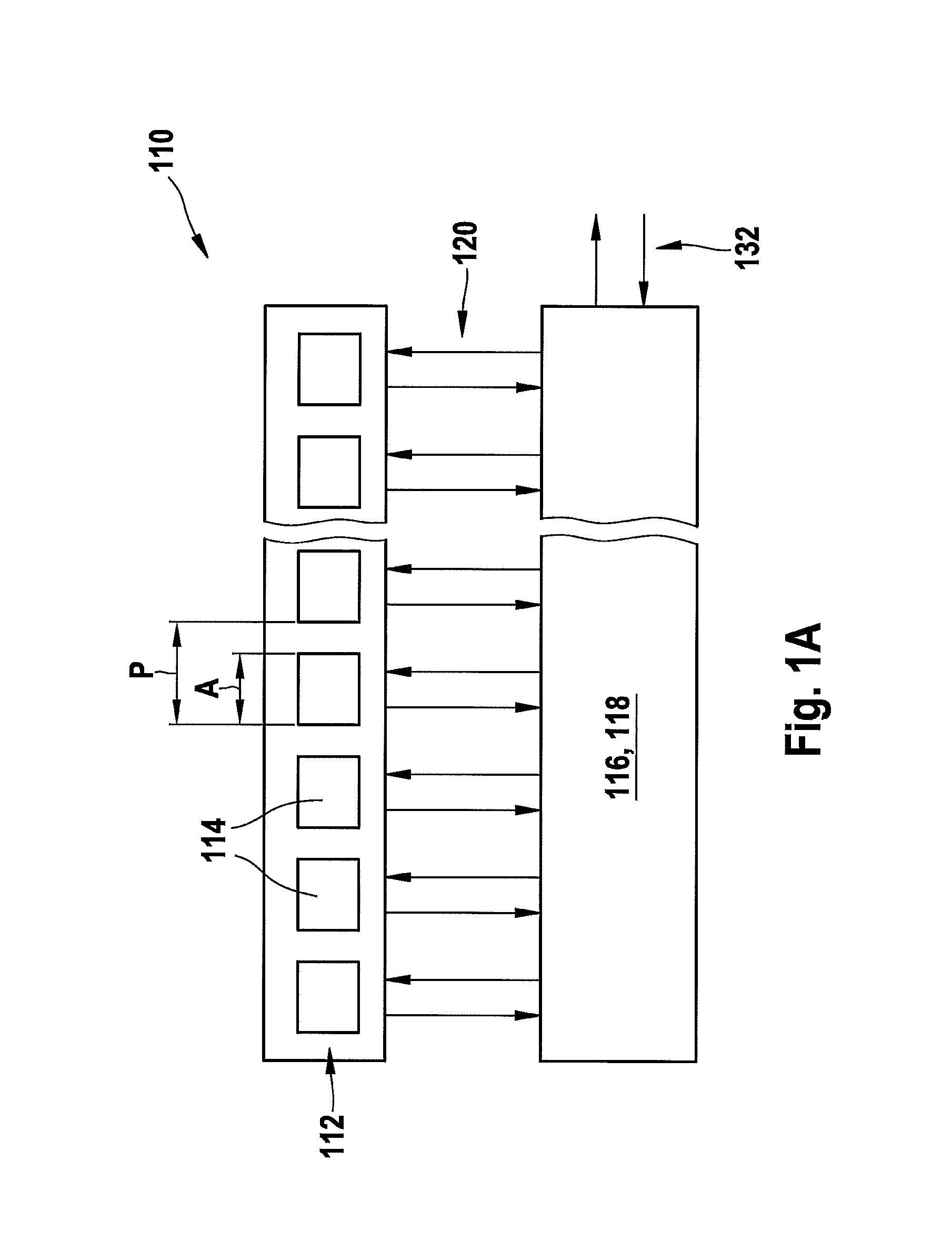
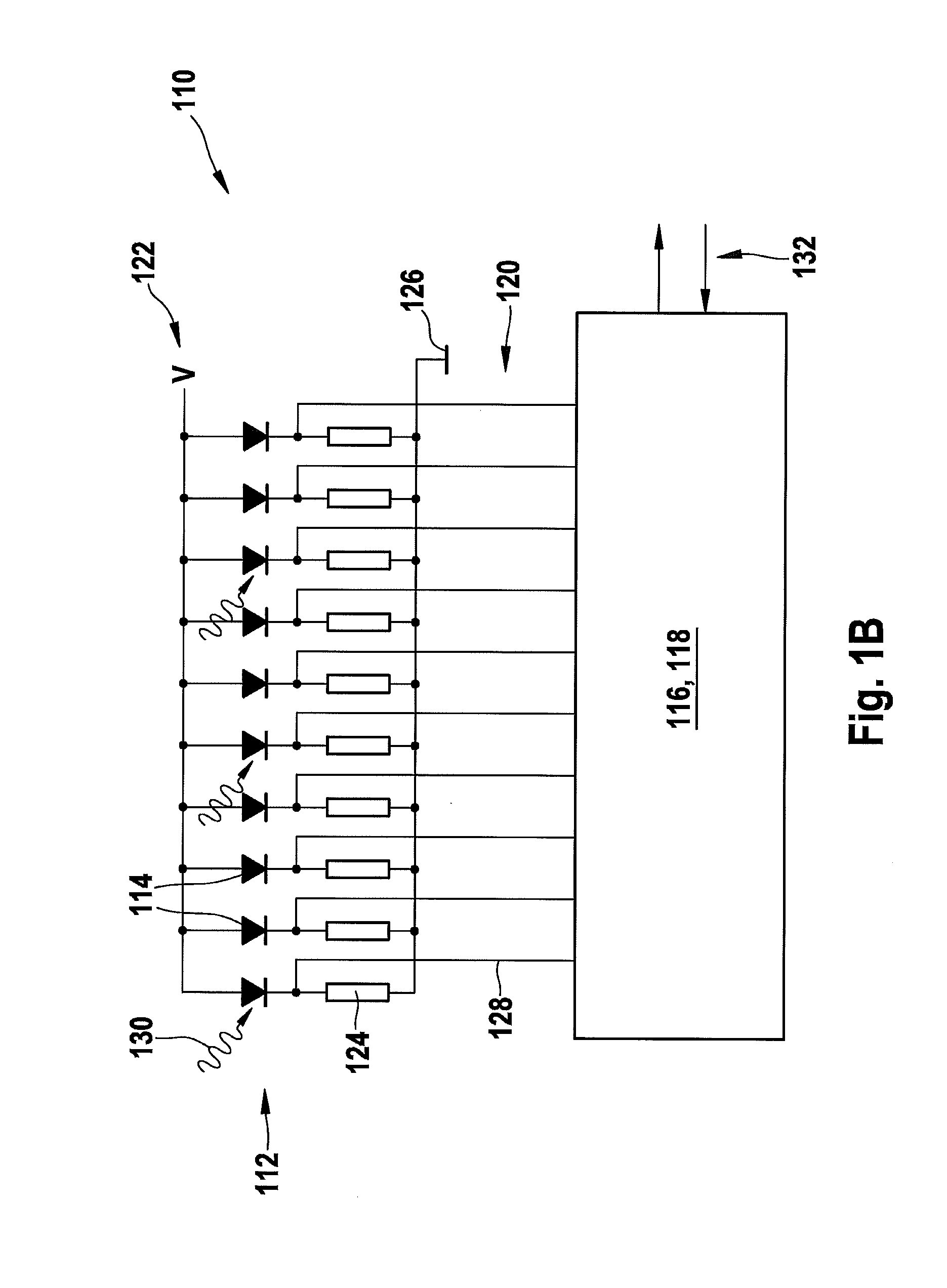
line array. An entire line of an image can be read out with high sensitivity and considerably reduced noise as compared to usual CCD arrays. It is also possible to detect single photons. Moreover the trigger circuit can be implemented such that as opposed to common CCD arrays all picture elements, i.e. all avalanche semiconductor diodes, can be read out at the same time. This results in a considerably increased detection speed.
[0029]This modification of the invention provides the
advantage that the active area of a picture element on an image line is now doubled and at the same time divided into two subareas (or more, depending on the number of line arrays) which can be read out independently. It is highly likely that during the
dead time of one avalanche
semiconductor detector the second avalanche
semiconductor detector is active, so that this second detector can continue to register photons. In this way the problem caused by dead times of avalanche semiconductor detectors is greatly reduced.
[0032]For any one of the above described accumulating or counting processes the parallel counter may in particular comprise a memory area including several memory cells. These memory cells can then be assigned to single avalanche semiconductor detectors of the line arrays or of one line array. Preset values (for example the preset value “1”) may be assigned to these memory cells, which preset values correspond to an idle state in which no signals are detected. The trigger circuit may then be configured to temporarily increase or lower the value of the
memory cell whenever one or more of the avalanche semiconductor detectors assigned to this
memory cell detect a light pulse. In case a single
photon is detected, for instance, the value of the
memory cell assigned to the avalanche
semiconductor detector which has detected the
photon can be lowered temporarily from the value “1” to the value “0”. The string of values of the memory cells which can be read out may then for example correspond to the image information of the line detector. Also accumulation can be easily carried out this way, for instance by accumulating those bit strings of the line array which have been registered during the counting time in a corresponding manner. Also the accumulation of a plurality of line arrays, for instance of two line arrays arranged in parallel, or the accumulation of the avalanche semiconductor detectors assigned to the same picture element on one line, respectively, can be easily realized in this manner. The values of the memory
cell can be reset to the original preset values after the detection has taken place and / or with a preset reading-out
clock rate so that the counting can start anew.
[0038]This is due to the fact that a coherent signal of the
sample area interferes in the
pupil plane of the spatial
beam splitter in such a manner that it generates the same structure in this plane as did the illumination signal irradiated before. An incoherent signal, on the other hand, is comprised of a plurality of
independent point emitters, each single one of which irradiates the entire
pupil plane of the spatial separation
beam splitter. The sum of all point emitters thus also irradiates the entire
pupil plane. This effect is used for separating the detection light coming from the sample into a coherent and a non-coherent part. The separation can be implemented with high efficiency and a high suppression ratio as well as at low cost.
[0040]The light detector described above comprising at least one line array and containing a plurality of avalanche semiconductor detectors can also be advantageously adapted in a scanning microscope such that different spectral wave length ranges of a
single area of the sample can be imaged onto different avalanche semiconductor detectors of the line array or of the light detector, respectively. This is particularly advantageous when two line arrays are used. For instance a
spectral separation element can be provided which separates image information of one line of the sample spectrally into at least two wave length ranges. These at least two wave length ranges may then be imaged onto different avalanche semiconductor detectors of the light detector. For instance a first wave length range may be imaged onto a first line array while a second wave length range may be imaged onto a second line array. In this case not only image information of one wave length range but image information of several wave length ranges may be acquired simultaneously at high speed, which may for instance have positive effects on the contrast or other
image properties. The microscope may e.g. be adapted such that a first line array acquires image information in a spectral range containing a first peak of a fluorescent colorant of the sample, while information in a range surrounding a second peak of a fluorescent colorant of the sample may be acquired by a second line array. For
spectral separation, various known
spectral separation elements may be used, such as gratings and / or prisms. Also in this preferred arrangement the suggested
highly sensitive light detector which can be read out quickly is particularly advantageous in that image information can be acquired simultaneously and with the highest sensitivity in different wave length ranges.
