Organic EL element having a partition with a step, method for manufacturing organic EL element, organic EL device, and electronic apparatus

a technology of organic el elements and partitions, which is applied in the direction of discharge tubes/lamp details, thermoelectric devices, discharge tubes, etc., can solve the problems of difficult formation of each layer in the laminated structure, unsuitable for generating different luminescent colors between adjacent organic el elements, and unsuitable for display devices

Active Publication Date: 2013-08-13
SEIKO EPSON CORP
View PDF6 Cites 5 Cited by
  • Summary
  • Abstract
  • Description
  • Claims
  • Application Information

AI Technical Summary

Benefits of technology

[0011]In this configuration, the step portion provided in the side wall of the partition wall serves as a measure for filling the film-forming region with the liquid. In addition, liquid repellency is imparted to the upper surface of the step portion, and the side wall has lyophilicity at the lower and upper sides of the step portion in comparison with the upper surface of the step portion. Therefore, a pinning position of the liquid can be securely separated into positions holding the step portion therebetween. Therefore, different organic thin films with stable sectional shapes after deposition can be formed on the lower and upper sides of the step portion to hold the step portion therebetween. That is, it is possible to provide an organic EL element including a functional layer having lower luminance variation and including different organic thin films with stable sectional shapes.
[0053]In this configuration, an organic EL device capable of achieving stable light emission characteristics can be provided because the device includes an organic EL element having lower luminance variation.

Problems solved by technology

That is, in fact, there is a problem that it is difficult to form each of the layers in the laminated structure-functional layer at a desired position in the height direction unless a region surrounded by the bank is uniformly filled with a predetermined amount of the thin-film material solution.
The configuration including the individual partition wall and the common partition wall described in Japanese Unexamined Patent Application Publication No. 2008-135255 is effective in forming a plurality of organic EL elements which produce a single luminescent color but is unsuitable for generating different luminescent colors between adjacent organic EL elements.
This configuration also has the problem of being unsuitable for a display device and the like which are aimed at securing a predetermined numerical aperture because the size and arrangement of a light-emitting region defined by the individual partition wall are limited by an arrangement relation to the common partition wall.

Method used


Image

  • Organic EL element having a partition with a step, method for manufacturing organic EL element, organic EL device, and electronic apparatus
  • Organic EL element having a partition with a step, method for manufacturing organic EL element, organic EL device, and electronic apparatus
  • Organic EL element having a partition with a step, method for manufacturing organic EL element, organic EL device, and electronic apparatus

Examples


first embodiment

Organic EL Device

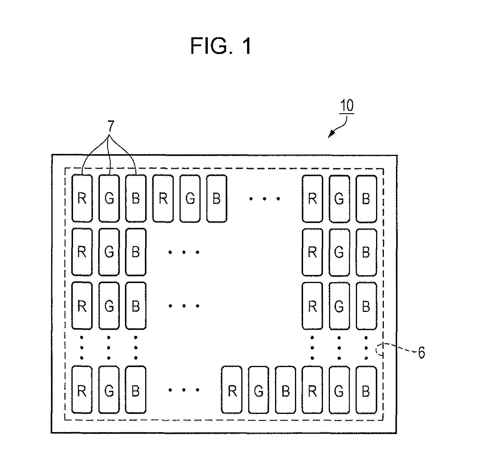
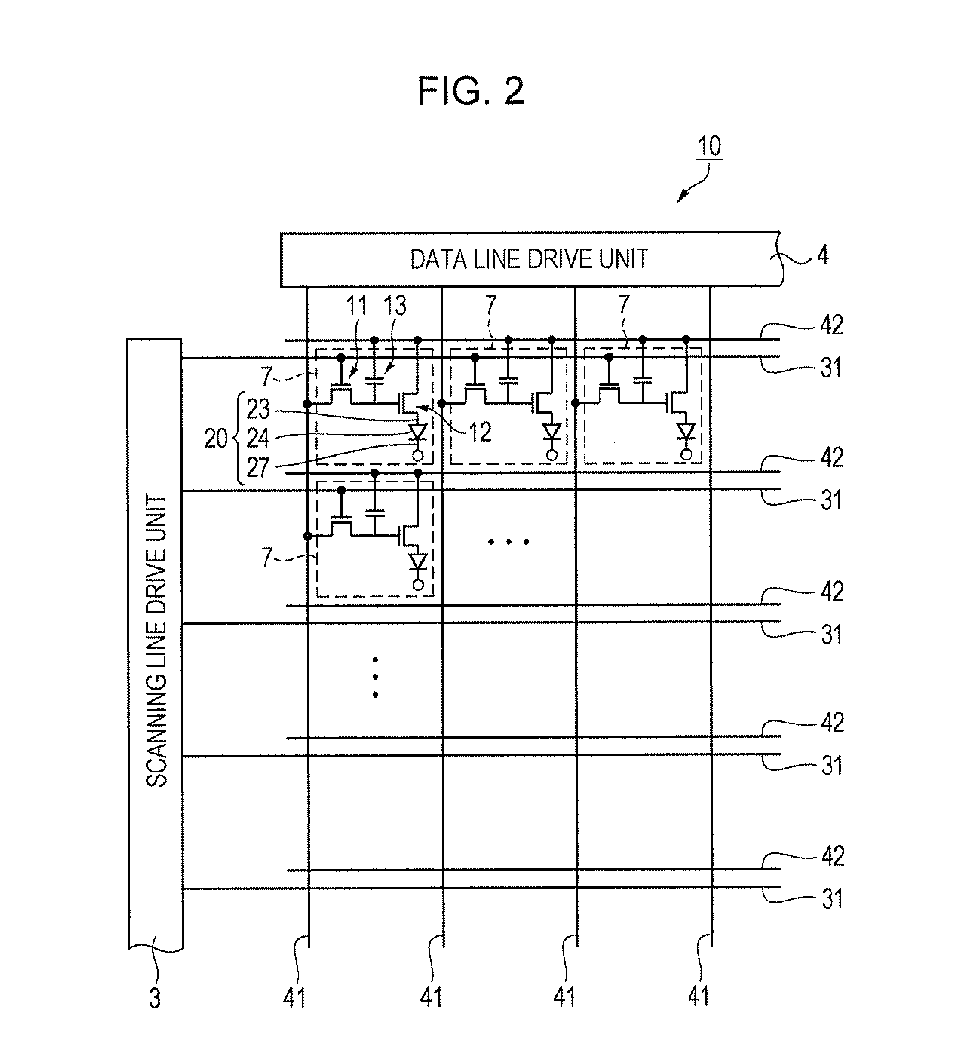
[0079]An organic EL device including an organic EL (Electroluminescence) element according to this embodiment is described with reference to FIGS. 1 to 3. FIG. 1 is a schematic front view showing a configuration of an organic EL device. FIG. 2 is an equivalent circuit diagram showing an electric configuration of an organic EL device. FIG. 3 is a schematic view showing a configuration of an organic EL element.

[0080]As shown in FIG. 1, an organic EL device 10 according to this embodiment includes light-emitting pixels 7 which emit lights (luminescent color) of red (R), green (G), and blue (B). The light-emitting pixels 7 have a substantially rectangular shape and are arranged in a matrix in a light-emitting region (display region) 6. The light-emitting pixels 7 which emit lights of the same color are arrayed in a vertical direction (column direction or longitudinal direction of light-emitting pixels) on the drawing. The light-emitting pixels 7 which emit lights of dif...

example 1

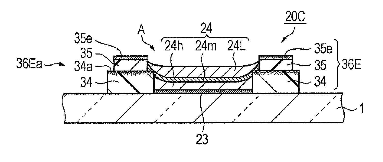
[0093]FIG. 4 is a schematic sectional view showing a structure of an organic EL element of Example 1. FIG. 5 is a flow chart showing a method for manufacturing the organic EL element of Example 1. FIGS. 6A to 6F and FIGS. 7G to 7K are schematic sectional views showing a method for manufacturing the organic EL element of Example 1.

[0094]As shown in FIG. 4, an organic EL element 20 of Example 1 includes a partition wall 36 which defines a pixel electrode 23 provided on an element substrate 1, a functional layer 24 provided in a film-forming region A defined by the partition wall 36, and a common electrode 27 provided to cover the functional layer 24 and the partition wall 36.

[0095]As the element substrate 1, a transparent glass or plastic substrate is used.

[0096]The pixel electrode 23 is formed using a transparent conductive film of ITO (Indium Tin Oxide) or the like, and the common electrode 27 is formed using a metallic material with reflectivity, such as opaque Al (aluminum) or the...

example 2

[0128]Next, an organic EL element of Example 2 and a method for manufacturing the same are described with reference to FIGS. 8 and 9A and 9B. FIG. 8 is a schematic sectional view showing a structure of an organic EL element of Example 2. FIGS. 9A and 9B are schematic sectional views each showing a structure of an organic EL element of a modified example of Example 2. In addition, the same components as in Example 1 are denoted by the same reference numerals and detail description thereof is omitted. In FIGS. 8 and 9A and 9B, a common electrode 27 is not shown.

[0129]An organic EL element of Example 2 utilizes the structure provided around the pixel element 23 in Example 2.

[0130]As shown in FIG. 8, an organic EL element 20 of Example 2 includes a pixel electrode 23 provided on an element substrate 1, a partition wall 36B which defines a film-forming region A including the pixel electrode 23 in two dimensions, and a functional layer 24 provided in the film-forming region A.

[0131]The pa...


PUM


Abstract

An organic EL element includes a functional layer disposed between an anode and a cathode on a substrate and including laminated different organic thin films including a light-emitting layer, and a partition wall which defines the functional layer. Each of the organic thin films is formed by applying a liquid containing a functional layer-forming material on a film-forming region defined by the partition wall and then drying the liquid. The partition wall has at least one step portion provided in the side wall thereof in the thickness direction, and liquid repellency is imparted to the uppermost surface of the partition wall and the upper surface of the step portion. The surface of the side wall excluding the step portion has lyophilicity in comparison with the upper surface of the step portion.

Description

BACKGROUND[0001]1. Technical Field[0002]The present invention relates to an organic EL (electroluminescence) element, a method for manufacturing an organic EL element, an organic EL device, and an electronic apparatus.[0003]2. Related Art[0004]An example of a method for manufacturing an organic EL element is disclosed, in which a functional layer including a light-emitting layer of an organic EL element is formed by a thin-film forming method of forming a thin-film layer by filling a region surrounded by a bank (partition wall) with a thin-film material solution (Japanese Unexamined Patent Application Publication. Nos. 11-271753 and 2008-135255).[0005]Japanese Unexamined Patent Application Publication No. 11-271753 discloses an example in which a functional layer includes a hole transport layer and an organic semiconductor layer (light-emitting layer). The bank has a laminated structure including an affinity layer showing affinity for the thin-film material solution (containing a ho...

Claims


Application Information

Patent Timeline
Patent Type & Authority Patents(United States)
IPC IPC(8): H01L29/08H01L35/24H01L51/00
CPCH01L27/3246H01L27/3283H01L51/0005H10K59/122H10K59/173H10K71/135
Inventor YANAGIHARA, HIROKAZU
Owner SEIKO EPSON CORP
Why Eureka
Try Eureka