Electronic component mounting structure, electronic component mounting method, and electronic component mounting board

a technology for electronic components and mounting structures, applied in the direction of printed circuits, sustainable manufacturing/processing, final product manufacturing, etc., can solve the problems of poor connection reliability, increased stress, and increased difficulty in ensuring connection reliability, so as to reduce the adhesion strength, suppress bad influences, and reduce the effect of stress reli

a technology for electronic components and mounting structures, applied in the direction of printed circuits, sustainable manufacturing/processing, final product manufacturing, etc., can solve the problems of poor connection reliability, increased stress, and increased difficulty in ensuring connection reliability, so as to reduce the adhesion strength, suppress bad influences, and reduce the effect of stress reli

US20100295177A1Active Publication Date: 2010-11-25NEC CORP

Image

  • Electronic component mounting structure, electronic component mounting method, and electronic component mounting board
  • Electronic component mounting structure, electronic component mounting method, and electronic component mounting board
  • Electronic component mounting structure, electronic component mounting method, and electronic component mounting board

Examples


Embodiment Construction

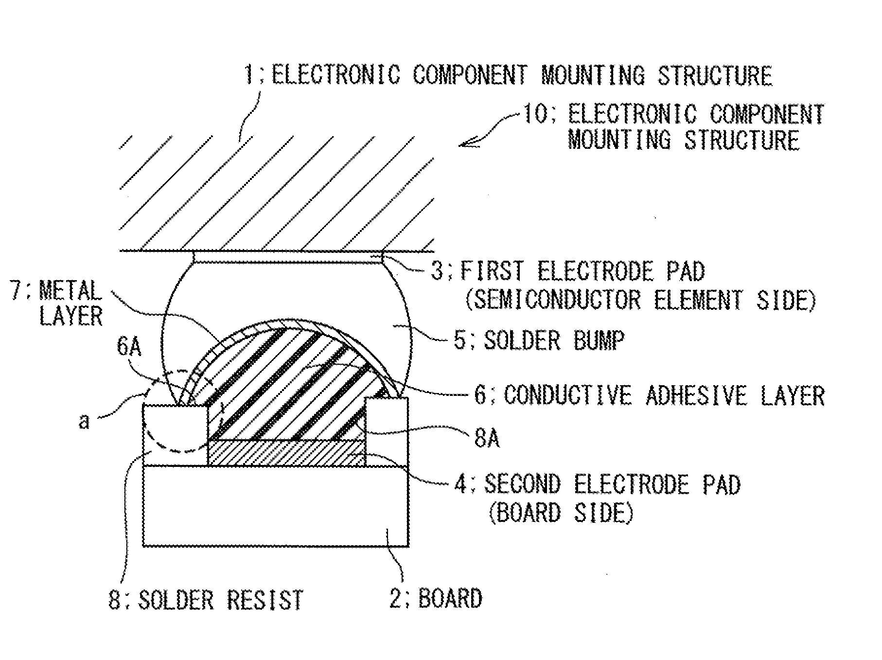
[0024]Referring to the accompanying drawings, an electronic component mounting structure according to the present invention will be described below. In an electronic component mounting structure 10 according to the present invention, a semiconductor element (electronic component) provided with electrode pads 3 and a board 2 provided with electrode pads 4 corresponding to the electrode pads 3 are arranged such that the electrode pads 3 and the electrode pads 4 are respectively opposed to each other. A solder bump 5 is formed on a surface of the electrode pad 3, and the electrode pad 3 and the electrode pad 4 are connected via a conductive adhesive layer 6 contacting the solder bump 5 and the electrode pad 4. Solder resist 8 having an opening 8A regulating an area of the electrode pad 4 is formed on a surface of the board 2, and the conductive adhesive layer 6 is formed to protrude from a surface of the solder resist 8. The conductive adhesive layer 6 has an elastic coefficient lower ...


PUM


Abstract

In an electronic component mounting structure, a semiconductor element (an electronic component) provided with an electrode pad and a board provide with an electrode pad corresponding to the electrode pad are connected via a conductive material portion. On a surface of the board, there is formed solder resist having an opening regulating an area of the electrode pad. The conductive material portion is formed to protrude from a surface of the solder resist. An elastic coefficient of the conductive material portion is lower than that of the solder resist. A solder bump and the conductive material portion are connected via a metal layer. The conductive material portion is formed to have an area larger than that of the opening of the solder resist. An edge of the conductive material portion is adhered to a portion of the surface of the solder resist. Thus, in a case of mounting an electronic component on a board by flip-chip connection, a reliability of connection can be secured.

Description

TECHNICAL FIELD[0001]The present invention relates to an electronic component mounting structure, an electronic component mounting method, and an electronic component mounting board.BACKGROUND ART[0002]As representative electronic components, there are known semiconductor elements such as a bare chip, a CSP (Chip-sized Package) and a BGA (Ball Grid Array) that are widely used in various kinds of electronic equipments. As electronic equipments rapidly develop, such semiconductor elements are required to have higher function than before. As a semiconductor element has higher function, a multi-pin configuration is required in accordance with increase in the number of input and output terminals of the semiconductor element, and a reduction in length of a signal transmission wiring is required in order to achieve a high-speed operation of the semiconductor element. A flip-chip connection is known as a mounting technique developed for accomplishing these requirements.[0003]The flip-chip c...

Claims


Application Information

Patent Timeline
25 Nov 2010
Publication
US20100295177A1
IPC
H01L23/48; H01L21/50; H05K1/11
CPC
H01L21/32; H01L2224/11334; H01L23/49811; H01L23/49816; H01L23/49866; H01L24/11; H01L24/13; H01L24/16
Inventors
OUCHI, AKIRA