Semiconductor pressure sensor and method of manufacturing the same

a technology of semiconductor pressure sensor and manufacturing method, which is applied in the direction of instruments, basic electric elements, measurement devices, etc., can solve the problems of difficult to downsize the semiconductor pressure sensor with high accuracy, the thickness of the diaphragm is apt to vary, etc., and achieve the effect of suppressing the variation in the performance of the semiconductor pressure sensor

Inactive Publication Date: 2013-08-27
MITSUBISHI ELECTRIC CORP
View PDF9 Cites 0 Cited by
  • Summary
  • Abstract
  • Description
  • Claims
  • Application Information

AI Technical Summary

Benefits of technology

[0007]It is an object of the present invention to provide a technique for suppressing the variation in the performance of a semiconductor pressure sensor, which is caused by downsizing.
[0009]The diaphragm body is formed of the multilayer structure which allows the control over the film thickness, the configuration, and the alignment with high accuracy. Therefore, it is possible to suppress the variation in the performance of the semiconductor pressure sensor, which is caused by downsizing. Since the diaphragm stopper protrudes, supporting the portion near the center of the diaphragm body which is apt to be distorted, this makes it possible to prevent the diaphragm body from being broken and allows thinning and downsizing of the diaphragm body. Further, since the polysilicon gauge resistor is disposed on the side of the vacuum chamber below the polysilicon diaphragm, the polysilicon gauge resistor resists being affected by the external environment. Therefore, a highly reliable semiconductor pressure sensor can be provided. Furthermore, by etching, the space in the diaphragm body is formed adjacently to the sacrificial layer. Therefore, since the flow of the etching solution or the like increases, it is possible to reduce the time required for the process steps of etching and the like and thereby reduce the time required for manufacturing the semiconductor pressure sensor.

Problems solved by technology

In such a manufacturing method, the thickness of the silicon substrate under the recess is controlled by the length of etching time, and this causes a problem that the thickness of the diaphragm is apt to vary.
Furthermore, since the variation in the amount of silicon of the substrate to be etched may cause misalignment between the gauge resistors and the recess, it is difficult to downsize the semiconductor pressure sensor with high accuracy.

Method used


Image

  • Semiconductor pressure sensor and method of manufacturing the same
  • Semiconductor pressure sensor and method of manufacturing the same
  • Semiconductor pressure sensor and method of manufacturing the same

Examples


Embodiment Construction

The First Preferred Embodiment

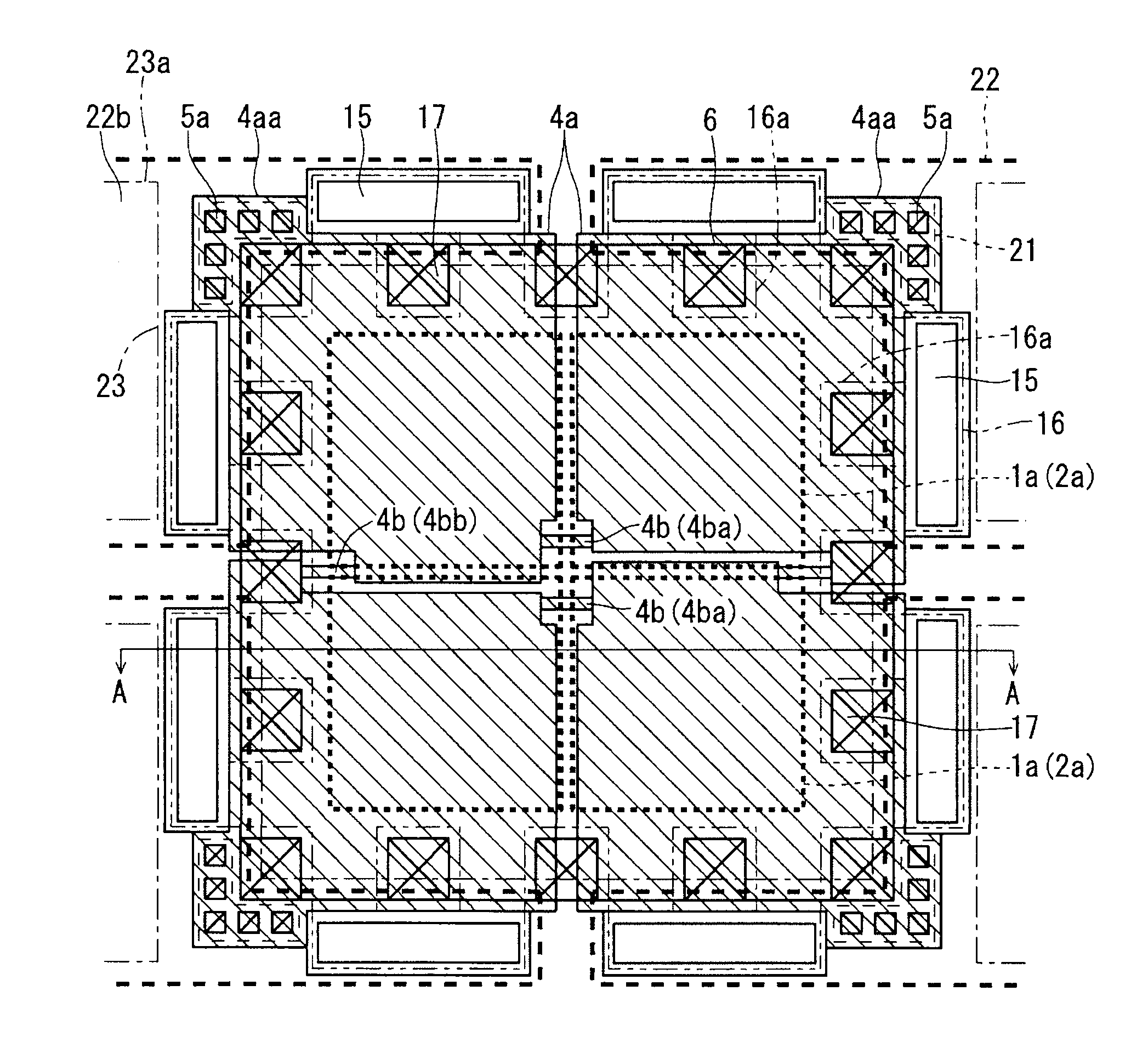
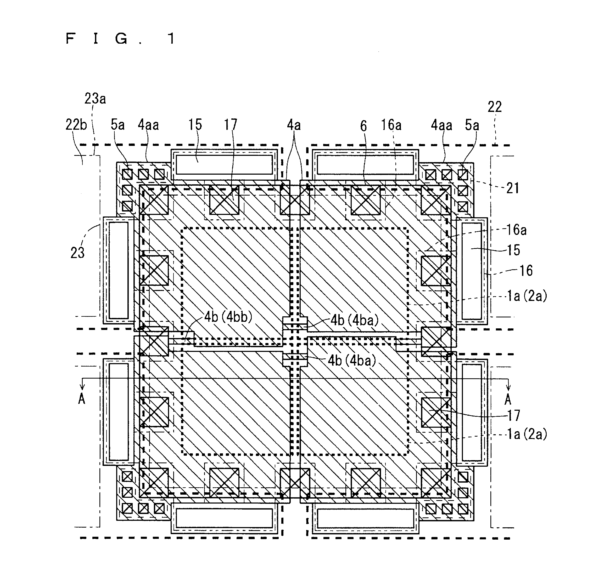
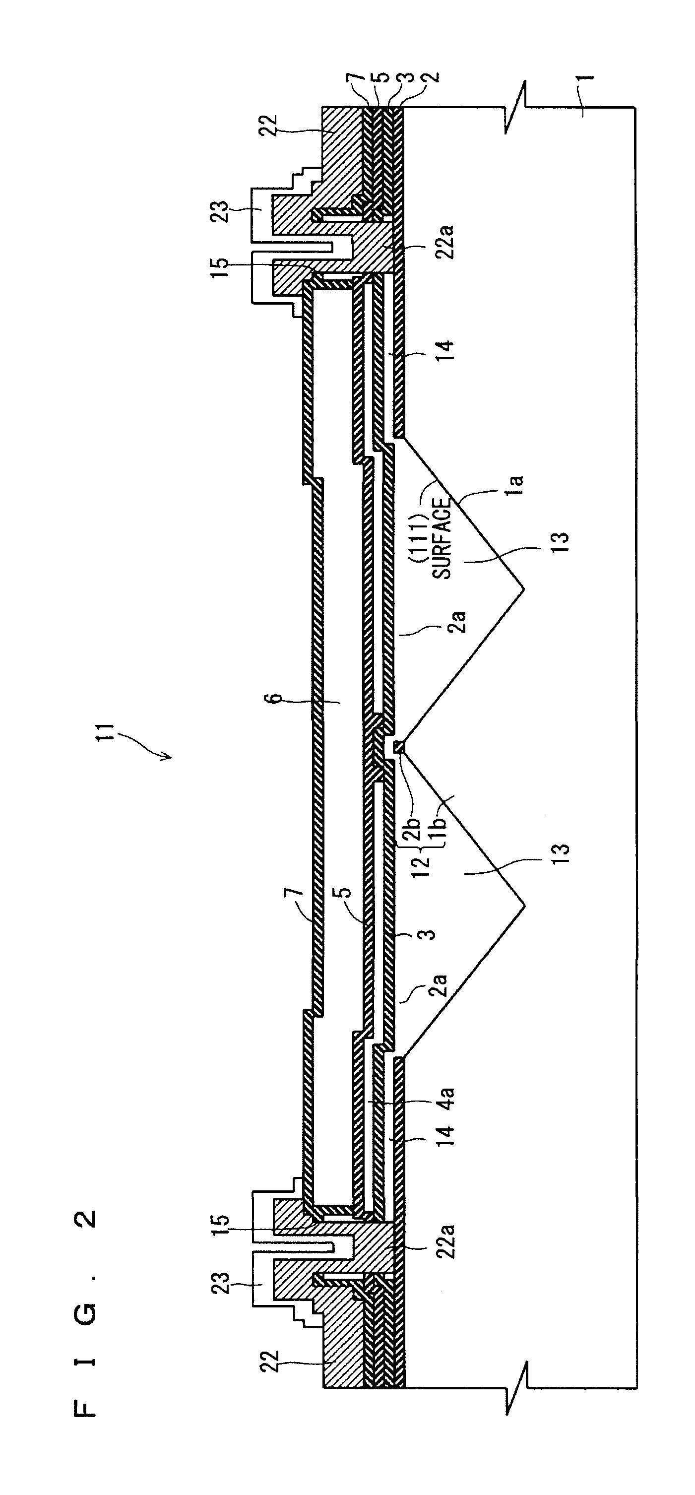
[0037]FIG. 1 is a plan view showing a semiconductor pressure sensor in accordance with the first preferred embodiment of the present invention, and FIG. 2 is a cross section taken along a line A-A of FIG. 1.

[0038]The semiconductor pressure sensor of the first preferred embodiment comprises a silicon substrate 1 which is a semiconductor substrate on which a plurality of (herein, four) recesses 1a are formed, a first insulating film 2 having a plurality of first openings 2a formed on the silicon substrate 1, a diaphragm body 11 formed of a multilayer structure, a first metal layer 21 (indicated by a thin broken line in FIG. 1), a second metal layer 22 (indicated by a thick broken line in FIG. 1), and a glass coat 23 (indicated by a thin one-dot chain line in FIG. 1).

[0039]The diaphragm body 11 includes a polysilicon wire 4a, a polysilicon gauge resistor 4b, a polysilicon diaphragm 6 formed above these elements 4a and 4b, and a group of insulating films co...


PUM

PropertyMeasurementUnit
widthaaaaaaaaaa
thicknessaaaaaaaaaa
thicknessaaaaaaaaaa

Abstract

In a method of manufacturing a semiconductor pressure sensor, a multilayer structure including a polysilicon diaphragm, a polysilicon gauge resistor formed on a side of a space which is to serve as a vacuum chamber below the polysilicon diaphragm, and a group of insulating films containing the polysilicon diaphragm and the polysilicon gauge resistor and having an etching solution introduction hole in contact with a sacrificial layer is formed on the sacrificial layer. Then, an etching solution is supplied through the etching solution introduction hole and the sacrificial layer is etched with the etching solution, to thereby obtain a diaphragm body formed of the multilayer structure, which functions on the vacuum chamber, and a surface of a silicon substrate below a first opening of a first insulating film is etched to thereby form the space which is to serve as the vacuum chamber and a diaphragm stopper disposed in the space, protruding toward near the center of the diaphragm body. With this structure, it is possible to provide a technique for suppressing the variation in the performance of a semiconductor pressure sensor when the semiconductor pressure sensor is downsized.

Description

BACKGROUND OF THE INVENTION[0001]1. Field of the Invention[0002]The present invention relates to a semiconductor pressure sensor and a method of manufacturing the same, and more particularly to a semiconductor pressure sensor including polysilicon gauge resistors and a method of manufacturing the same.[0003]2. Description of the Background Art[0004]As a type of pressure sensor, a semiconductor pressure sensor using a semiconductor substrate is used. In such a semiconductor pressure sensor, a plurality of diffused resistors serving as gauge resistors of which the resistance varies in accordance with pressure applied thereto are formed on a surface of a silicon substrate and the diffused resistors are bridged by diffusion wires of which the resistance value is low. The gauge resistors are arranged, for example, at respective portions of four sides of a rectangular diaphragm (thin film). On the other hand, on a surface of the silicon substrate which is opposite to the region in which t...

Claims


Application Information

Patent Timeline
Patent Type & Authority Patents(United States)
IPC IPC(8): G01L9/00B23P23/00H01L21/00
CPCG01L9/0054Y10T29/49
Inventor SATO, KIMITOSHI
Owner MITSUBISHI ELECTRIC CORP
Why Eureka
Try Eureka