Optical module stress release method

A stress release, optical module technology, applied in the field of optical communication, can solve problems such as failure, optical module power and performance changes, incomplete optical module stress release, etc., to ensure stability and reliability, process simplicity, and avoid power deviation. and the effect of changes in performance

Active Publication Date: 2019-09-06
DALIAN CANGLONG OPTOELECTRONICS TECH
View PDF6 Cites 2 Cited by
  • Summary
  • Abstract
  • Description
  • Claims
  • Application Information

AI Technical Summary

Problems solved by technology

[0004] The purpose of the present invention is to solve the problem that the incomplete stress release of the optical module will lead to changes in the power and performance of the optical module, resulting in the performance of the optical module not meeting the requirements or failure, and to provide a stress release method for the optical module that can completely release the stress , the optical modules can be screened to remove products with large performance changes

Method used


Image

  • Optical module stress release method
  • Optical module stress release method
  • Optical module stress release method

Examples


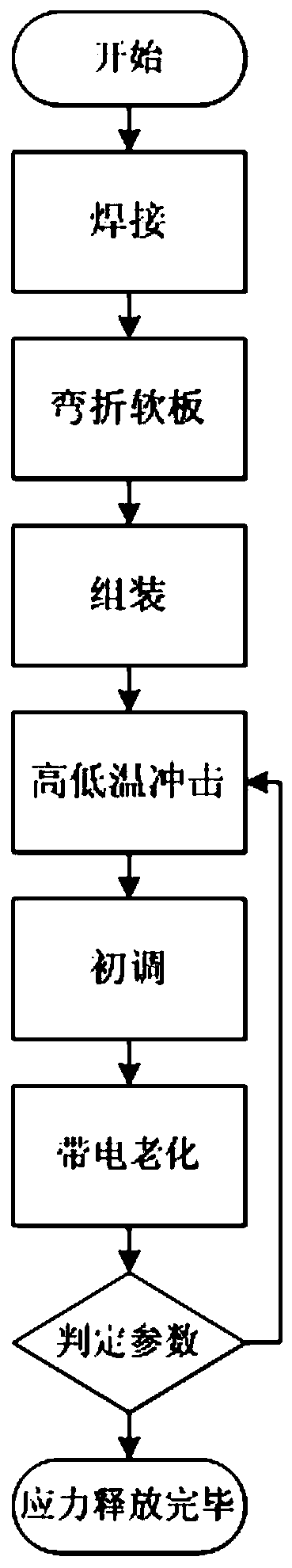
specific Embodiment approach 1

[0020] (1) Soldering: Use Weller PUD 81 welding workbench with a power of 95W, adjust the temperature of the soldering iron to 360-380°C, and use lead-free solder wire with a diameter of 0.5mm to solder the optical device to the PCBA board of the optical module through the soft board. Welding time for each solder spot shall not exceed 3 seconds;

[0021] (2) Bending the flexible board: the size of the flexible board is greater than 12mm, and the distance between the bottom of the device and the PCBA board is less than 2mm. The flexible board is bent into an S shape. Where the flexible board bends, the arc radius must be ≥ 1mm.

[0022] (3) Assembly: Place the optical device, bent soft board and PCBA board into the optical module casing, put the snap ring of the optical device pin into the corresponding position of the optical module casing, and adjust the optical device and PCBA board Arrive at the proper position, and visually observe whether the PCBA board is parallel to the...

specific Embodiment approach 2

[0028] This embodiment adopts basically the same processing method as in Example 1, the difference is (2) bending the soft board: the size of the soft board is less than 10mm, and the distance from the bottom of the device to the PCBA is greater than 3mm, and the soft board is bent into a U shape. Where the corner is turned, it is necessary to satisfy the arc radius ≥ 1mm.

specific Embodiment approach 3

[0030] This embodiment uses basically the same processing method as in Embodiment 1, the difference is (2) Bending the flexible board: use a simple and intuitive judgment method to bend the flexible board, first bend the flexible board into a U shape, and then place it in the optical module In the casing, observe the soft board when installing the top cover. If the U-shaped bend is flattened, the soft board needs to be bent into an S-shape; otherwise, the U-shape meets the requirements.

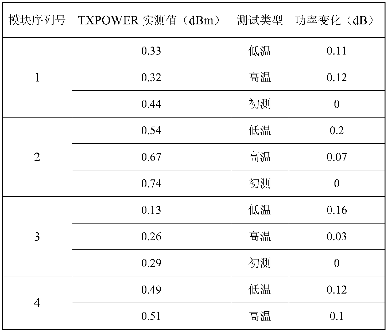
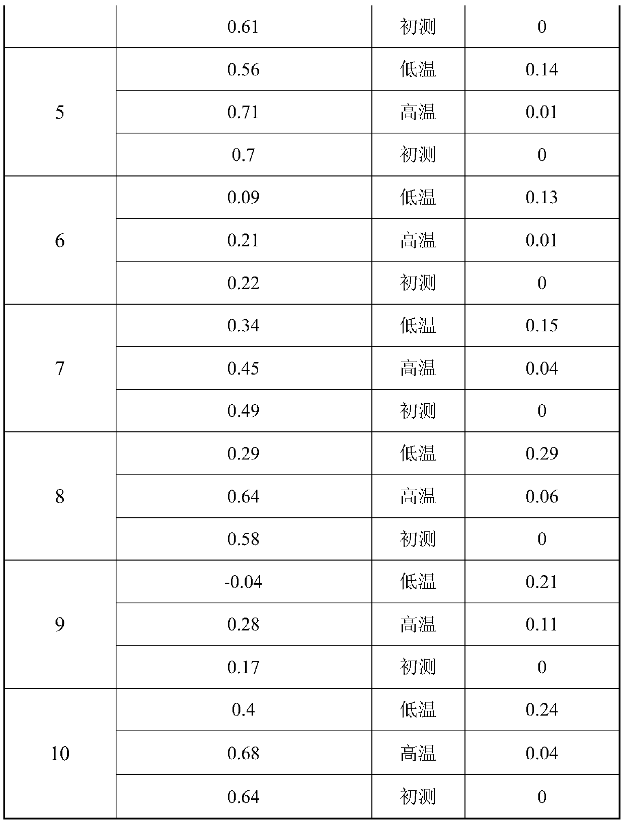
[0031] Table 1 Comparison of test results before and after stress release of optical modules

[0032]

[0033]

[0034] Using the stress release method of the optical module described in the above embodiment, the test results in Table 1 can be achieved by bending the flexible board into an S-shape or a U-shape. The data in the table are the initial adjustment and final inspection test data at room temperature 25°C It can be seen from the power changes in the table that the power changes...


PUM

PropertyMeasurementUnit
diameteraaaaaaaaaa

Abstract

The invention relates to the field of optical communication, in particular to a production process of an optical module. An optical module stress release method comprises the following steps: (1) welding an optical device; (2) bending a soft plate; (3) assembling the optical module; (4) performing rapid high-low temperature impact on the optical module; (5) performing normal temperature initial adjustment on the performance of the optical module; (6) electrically aging the optical module; and (7) carrying out a final detection test on the optical module, and comparing parameters such as power,current and reported value of normal temperature initial adjustment to check whether the stress release is complete. With the method, the stress generated when the optical device is welded and the soft plate is bent and the stress generated when the optical device, the soft plate and a PCBA plate are assembled into a tube shell can be effectively released, and the variation of power deviation andperformance caused by the stress of the optical device in the tube shell of the optical module is avoided, so that the stability and reliability of the optical module are guaranteed. The process is simple and convenient, and the method is suitable for the optical modules in various packaging forms.

Description

technical field [0001] The invention relates to the field of optical communication, in particular to a production process of an optical module. Background technique [0002] With the rapid development of the optical communication industry, the application of optical modules is becoming more and more extensive. Optical modules are the core components of optical communication. Optical modules include laser transmitters, laser receivers, PCBA and shells, which mainly complete the transmission of optical signals. And receiving, when the optical module enters the communication network, the customer is most concerned about its stability and reliability. The stress of the optical module mainly comes from the welding and assembly of the optical device and PCBA between the optical device shell and the module shell. Stress, if the stress is not released completely, it will lead to changes in the power and performance of the optical module, resulting in the performance of the optical m...

Claims


Application Information

Patent Timeline
Patent Type & Authority Applications(China)
IPC IPC(8): C21D9/50C21D10/00
CPCC21D9/50C21D10/00
Inventor 崔琳崔晓磊倪晓珍张文臣张彩
Owner DALIAN CANGLONG OPTOELECTRONICS TECH
Why Eureka
Try Eureka