

Wafer-level lens array, method of manufacturing wafer-level lens array, lens module and imaging unit
a technology of wafer-level lenses and lens modules, which is applied in the field of wafer-level lens arrays, can solve the problems of large deformation of the lens surface, large deformation of the lens unit, and large deformation of the resin, so as to prevent the positional deviation, prevent the deterioration of image quality, and design easy
- Summary
- Abstract
- Description
- Claims
- Application Information
AI Technical Summary
Benefits of technology
Problems solved by technology
Method used
Image

Examples
Embodiment Construction
[0045]First, the structure of a wafer-level lens array, a lens module, and an imaging unit according to an embodiment of the invention will be described.
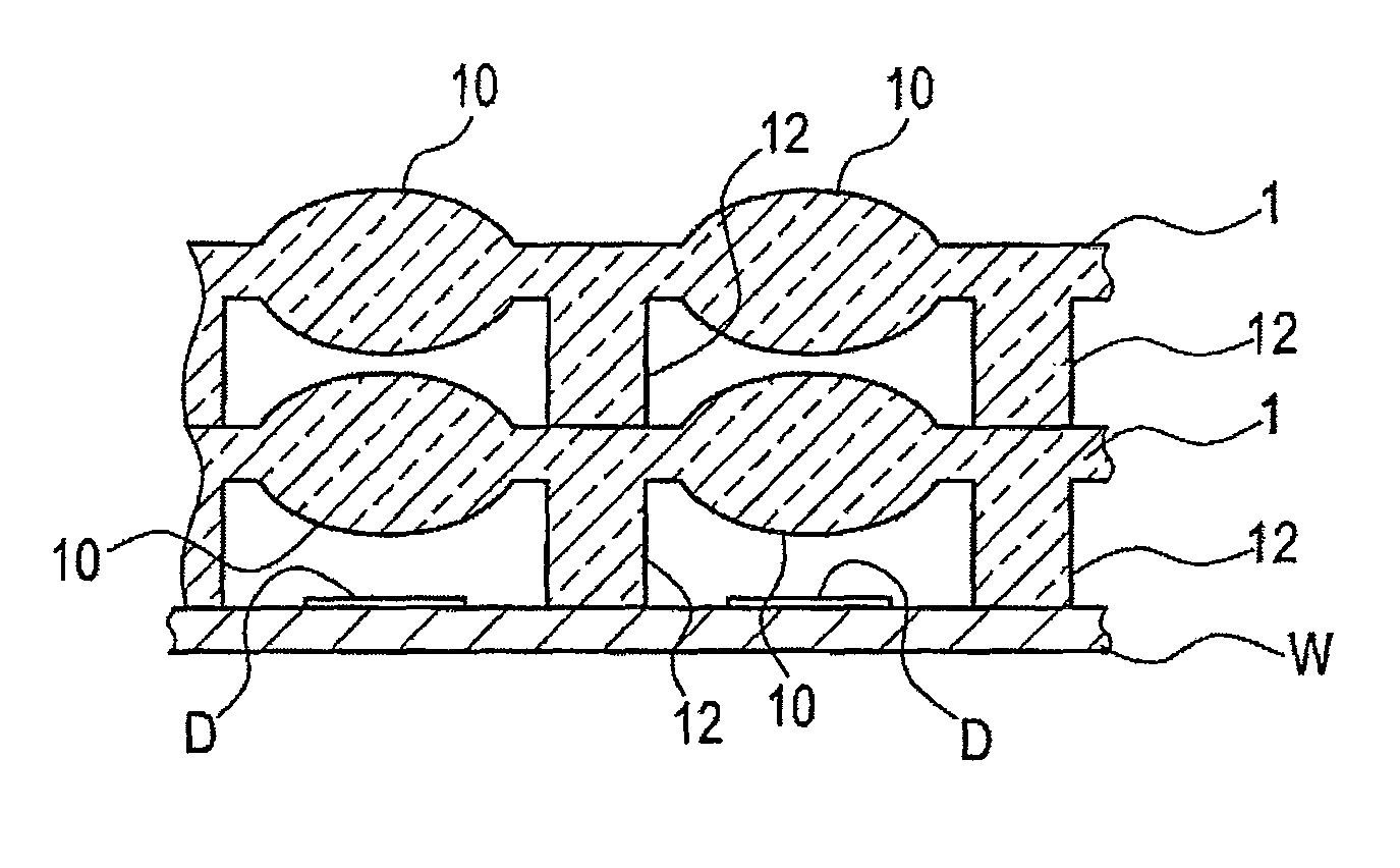
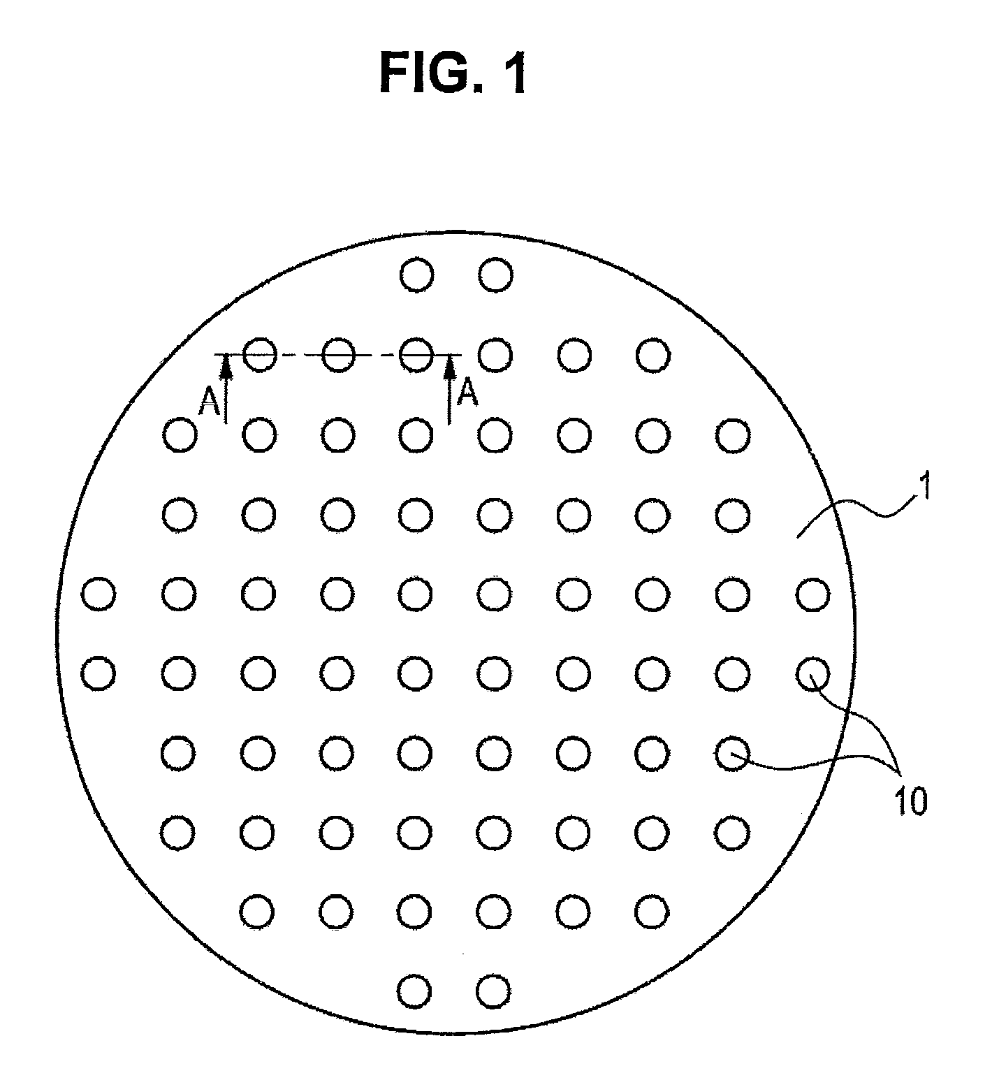
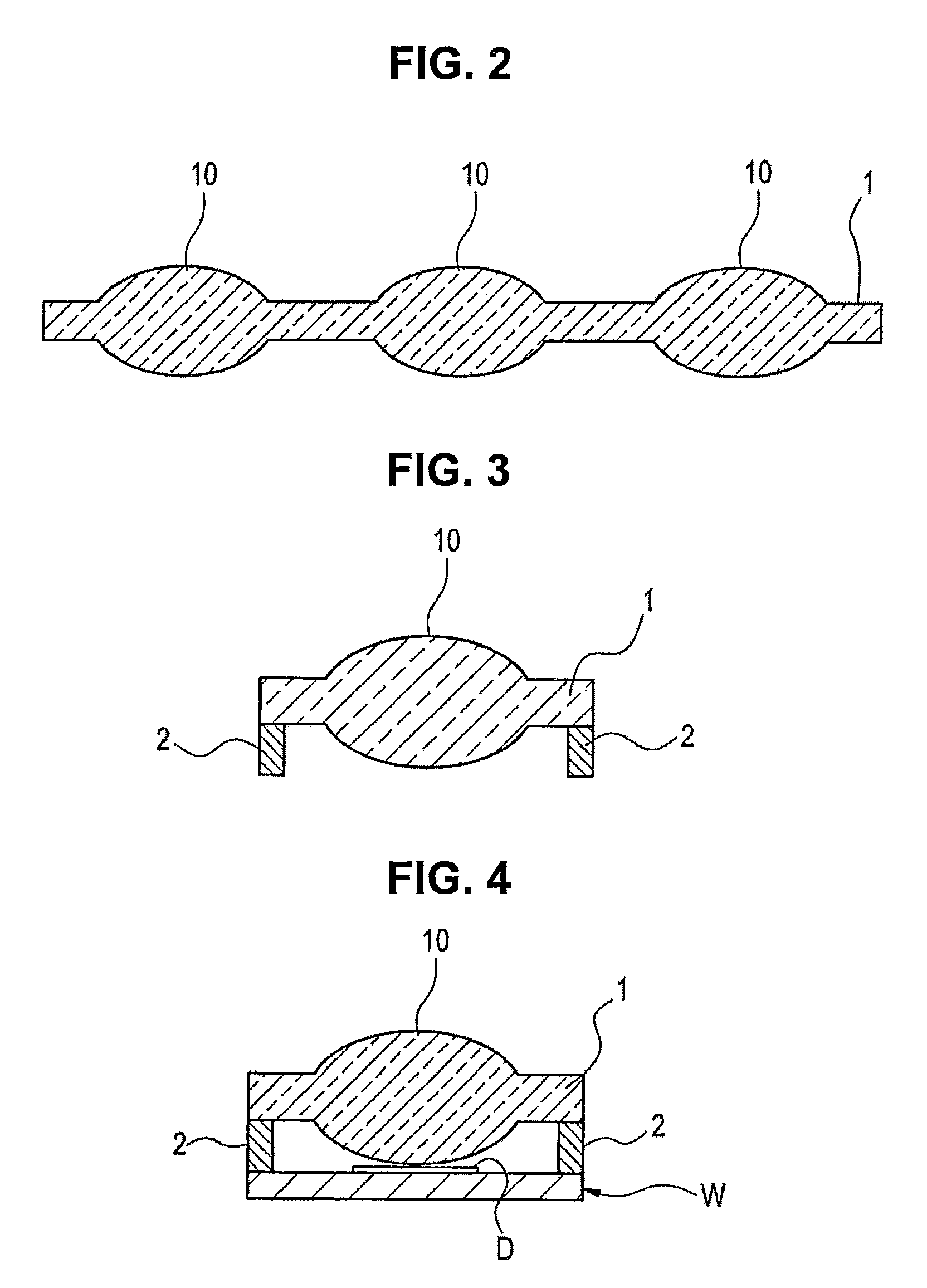
[0046]FIG. 1 is a plan view illustrating an example of the structure of the wafer-level lens array. FIG. 2 is a cross-sectional view illustrating the wafer-level lens array taken along the line A-A of FIG. 1.
[0047]The wafer-level lens array includes a substrate unit 1 and a plurality of lens units 10 that is arranged on the substrate unit 1. The plurality of lens units 10 is one-dimensionally or two-dimensionally arranged on the substrate unit 1. In this embodiment, as shown in FIG. 1, an example of the structure in which the plurality of lens units 10 is two-dimensionally arranged on the substrate unit 1 will be described. The lens units 10 are made of a resin that has substantially the same optical characteristics as that forming the substrate unit 1 and are formed integrally with the substrate unit 1. The shape of the lens unit 1...
PUM
| Property | Measurement | Unit |
|---|---|---|
| Abbe numbers | aaaaa | aaaaa |
| Abbe numbers | aaaaa | aaaaa |
| Abbe number | aaaaa | aaaaa |
Abstract
Description
Claims
Application Information