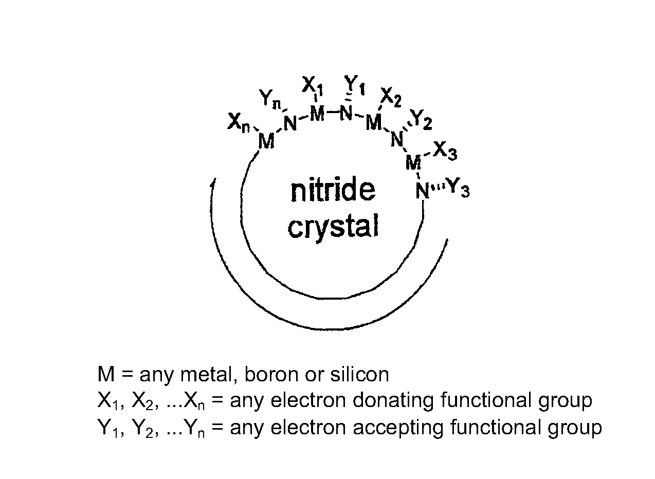
Nanoparticles

a technology of semiconductor nanoparticles and nanoparticles, which is applied in the direction of luminescent compositions, polycrystalline material growth, crystal growth process, etc., can solve the problems of weak emissivity of materials, poor control of the size of nanocrystals produced, and light strong emission that has never been reported in nitride nanocrystal preparations, etc., to achieve strong emission, low cost, and pronounced quantum size effects

Inactive Publication Date: 2013-10-08
SHARP KK
View PDF36 Cites 6 Cited by
  • Summary
  • Abstract
  • Description
  • Claims
  • Application Information

AI Technical Summary

Benefits of technology

[0022]The light-emissive nitride nanoparticle may comprise: a nitride crystal, at least one dimension of the crystal being of a nanoscale dimension; and at least one capping agent provided on a surface of the nitride crystal and containing an electron-accepting group for passivating nitrogen atoms at the surface of the crystal. The emissive nitride nanocrystals of the invention have been prepared for the first time by performing the synthesis of a metal nitride in the presence of capping agents which are able to coordinate effectively to the surface of the growing crystal. It has been found that providing a capping agent having an electron-accepting group significantly increases the quantum yield of the resultant nitride nanoparticle—prior art nitride nanoparticles have a photoluminescence quantum yield of well below 1%, whereas nitride nanoparticles manufactured by a method of the present invention can have a photoluminescence quantum yield of 20% or greater.
[0026]The at least one capping agent may further contain an electron-donating group for passivating metal, boron or silicon atoms at the surface of the crystal or the nitride layer. This may help to promote solubility of one or more constituents in the reaction mixture during growth of the nanocrystals, thereby to provide a more homogeneous solution which should allow for more controlled growth of the nanocrystals.
[0028]The electron-accepting group may include a metal, boron or silicon. Such an electron-accepting group has been found to be effective in the manufacture of a nitride nanoparticle with a high quantum yield.
[0041]It is believed that the zinc atom in the zinc stearate is able to coordinate to the nitrogen atoms on the surface of the nanocrystal which allows controlled growth of the nanocrystals and also passivates the surface and provides strong emission. This provides a significant advantage over the prior art.
[0042]Compared to other semiconductors the nitrides span a wider range of the electromagnetic spectrum and like other III-V materials they have large exciton diameters suggesting they should have more pronounced quantum size effects on the optical spectra [Brus, J. Chem. Phys., 1983, 33, 6976]. This property is seen in the emission spectra of indium nitride nanocrystals prepared using the current invention shown in FIG. 2 which shows tunability over at least the range from 480 nm to 850 nm which is a larger range than nanocrystals made from any other material known in the prior art. At the present time the majority of emissive nanocrystals are composed of II-VI materials such as cadmium sulphide, cadmium selenide and lead sulphide. The presence of highly toxic heavy metals in these materials also gives the nitride nanocrystals of the present invention a significant advantage over the prior art. Ever tightening regulations and consumer awareness make using toxic materials in consumer products increasingly difficult. Another advantage is the low cost of all the starting materials used to prepare the nitride nanocrystals described here and the simple one step process used to prepare the nanocrystals from these materials.

Problems solved by technology

However, to date, routes to fabricate nitride nanocrystals have resulted in only weakly emissive materials and have had poor control over the size of the nanocrystals produced.
Other workers have attempted to prepare nitride nanocrystals in the presence of capping agents, but strong emission of light has never been reported in nitride nanocrystals prepared in these ways.

Method used


Image

  • Nanoparticles
  • Nanoparticles
  • Nanoparticles

Examples


example 1

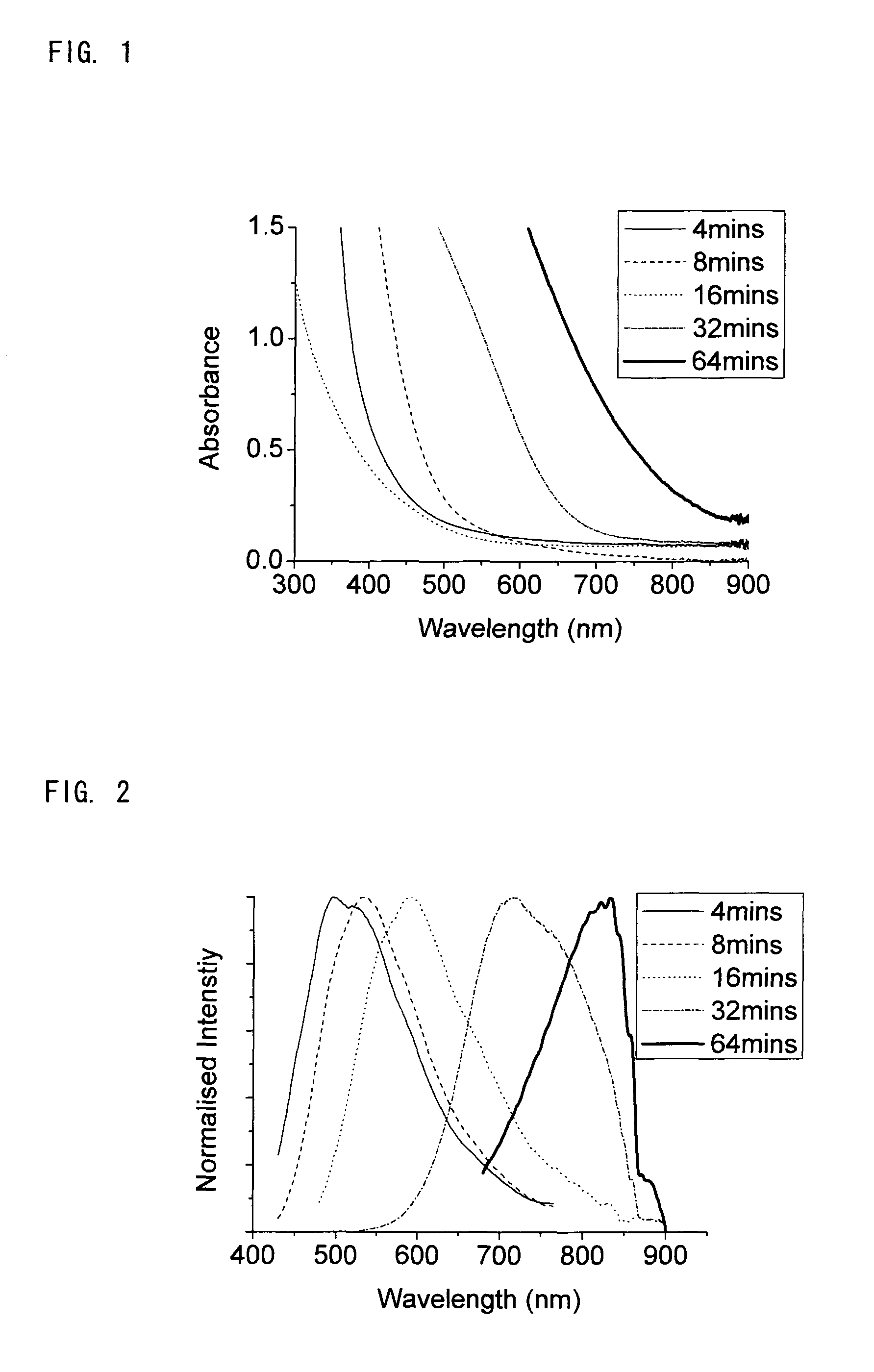
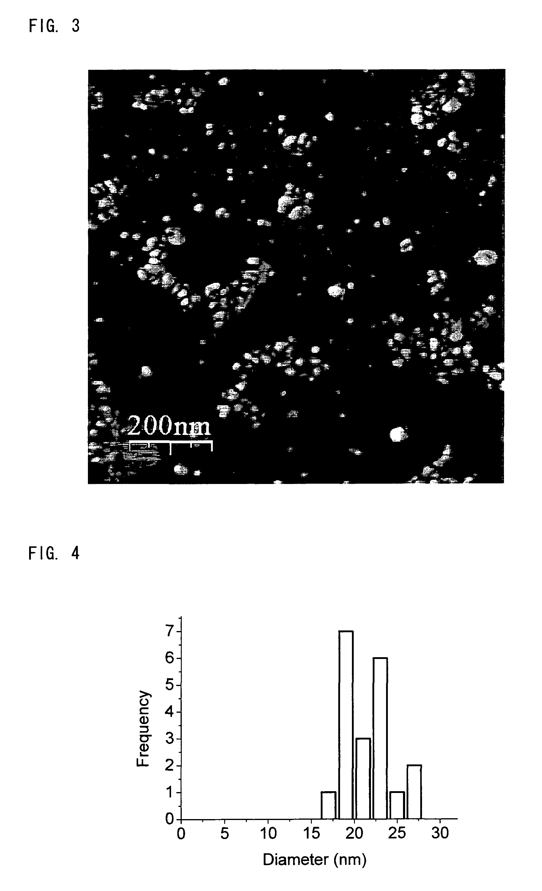
[0105]Indium iodide (300 mg, 0.6 mmol), sodium amide (500 mg, 12.8 mmol), hexadecane thiol (308 μl, 1.0 mmol), zinc stearate (379 mg, 0.6 mmol) and diphenyl ether (20 ml) were heated rapidly to 225° C. Of the constituents, Indium iodide provided a Group III metal (Indium), sodium amide provided nitrogen, hexadecane thiol is a capping agent with an electron-donating group, zinc stearate is a capping agent with an electron-accepting group and diphenyl ether acts as a solvent. Over the course of 60 minutes a number of 0.25 ml portions of the reaction mixture were removed and diluted with cyclohexane (3 ml) and any insoluble materials were removed using a centrifuge. The resulting clear solutions were analysed by absorption and emission spectroscopy and showed a change in the maximum emission wavelength from 480-850 nm over the course of the reaction, as shown in FIGS. 1 and 2. The peak in the emission spectrum has a full width at half the maximum intensity of the order of 150 nm.

[0106]...

example 2

[0113]Indium iodide (300 mg, 0.6 mmol), sodium amide (500 mg, 12.8 mmol), hexadecane thiol (308 μl, 1.0 mmol), zinc stearate (379 mg, 0.6 mmol) and diphenyl ether (20 ml) were heated rapidly to 250° C. Over the course of 40 minutes 0.25 ml portions of the reaction mixture were removed and diluted with cyclohexane (3 ml) and any insoluble material was removed using a centrifuge. This gives clear solutions of emissive indium nitride nanocrystals. As in example 1, the absorption / emission properties of the obtained nanoparticles depend on the reaction, and show a similar dependence on time to FIGS. 1 and 2.

example 3

[0114]Indium iodide (300 mg, 0.6 mmol), sodium amide (500 mg, 12.8 mmol), palmitic acid (256.4, 1.0 mmol), zinc stearate (379 mg, 0.6 mmol) and diphenyl ether (20 ml) were heated rapidly to 225° C. In this example, palmitic acid is used as a capping agent with an electron-donating group rather than hexadecane thiol.

[0115]Over the course of 40 minutes 0.25 ml portions of the reaction mixture were removed and diluted with cyclohexane (3 ml) and any insoluble material was removed using a centrifuge. This gives clear solutions of indium nitride nanocrystals. As in example 1, the absorption / emission properties of the obtained nanoparticles depend on the reaction, and show a similar dependence on time to FIGS. 1 and 2.


PUM

PropertyMeasurementUnit
photoluminescence quantum yieldaaaaaaaaaa

Abstract

The present application provides a light-emissive nitride nanoparticle, for example a nanocrystal, having a photoluminescence quantum yield of at least 1%. This quantum yield is significantly greater than for prior nitride nanoparticles, which have been only weakly emissive and have had poor control over the size of the nanoparticles produced. The nanoparticle includes at least one capping agent provided on a surface of the nitride crystal and containing an electron-accepting group for passivating nitrogen atoms at the surface of the crystal. The invention also provides non-emissive nitride nanoparticles.

Description

TECHNICAL FIELD[0001]This invention relates to semiconductor nanoparticles, for example nanocrystals having nanometer dimensions, and in particular to such materials in a nitride material system. Such materials can be used in a wide range of applications including phosphor-converted LEDs, emissive EL displays, solar cells and bio-imaging.BACKGROUND ART[0002]Semiconductor nanocrystals whose dimensions are comparable to the bulk exciton diameter show quantum confinement effects. This is seen most clearly in the optical spectra which shift to blue wavelengths as the size of the crystal is reduced.[0003]Semiconductor nanocrystals made from a wide range of materials have been studied including many II-VI and III-V semiconductors. In addition to spherical nanocrystals, rod-, arrow-, teardrop- and tetrapod-shaped nanocrystals [Alivisatos et al., J. Am. Chem. Soc, 2000, 122, 12700; WO03054953] and core-shell structures [Bawendi, J. Phys. Chem. B, 1997, 101, 9463; Li and Reiss, J. Am. Chem. ...

Claims


Application Information

Patent Timeline
Patent Type & Authority Patents(United States)
IPC IPC(8): H01L33/06
CPCB82Y30/00C01B21/06C01B21/0632C09K11/025C09K11/62C30B7/06C30B29/38C30B29/403C30B29/60C01B21/064C01B21/068C01B21/072C01P2002/72C01P2002/74C01P2004/04C01P2004/64C01P2004/84C01G15/00
Inventor TAYLOR, PETER NEILHEFFERNAN, JONATHAN
Owner SHARP KK
Why Eureka
Try Eureka