Semiconductor device

a technology of semiconductors and transistors, applied in the direction of semiconductor devices, basic electric elements, electrical equipment, etc., can solve the problems of deteriorating the long-term reliability of the device, and achieve the effect of enhancing the long-term reliability of the transistor

Active Publication Date: 2013-10-08
RENESAS ELECTRONICS CORP
View PDF16 Cites 15 Cited by
  • Summary
  • Abstract
  • Description
  • Claims
  • Application Information

AI Technical Summary

Benefits of technology

[0015]This configuration makes it possible to cover the lower corner of the trench, on the drain side, with the second low-concentration region and to locate a PN boundary line at a position distant from the lower corner of the trench on the drain side. Even when a voltage is applied to the gate electrode and drain electrode upon operation of a transistor to apply a predetermined voltage between the second low-concentration region and the channel region, electric field concentration to the lower corner of the trench can be prevented. This prevents generation of hot carriers and as a result, the long term reliability of the transistor is enhanced.

Problems solved by technology

The present inventors have however found that a problem occurs in a transistor having such a configuration in which a source region and a drain region are extended to the vicinity of the bottom portion of a gate electrode.
Generation of such hot carriers deteriorates the long term reliability of the device.

Method used


Image

  • Semiconductor device
  • Semiconductor device
  • Semiconductor device

Examples


first embodiment

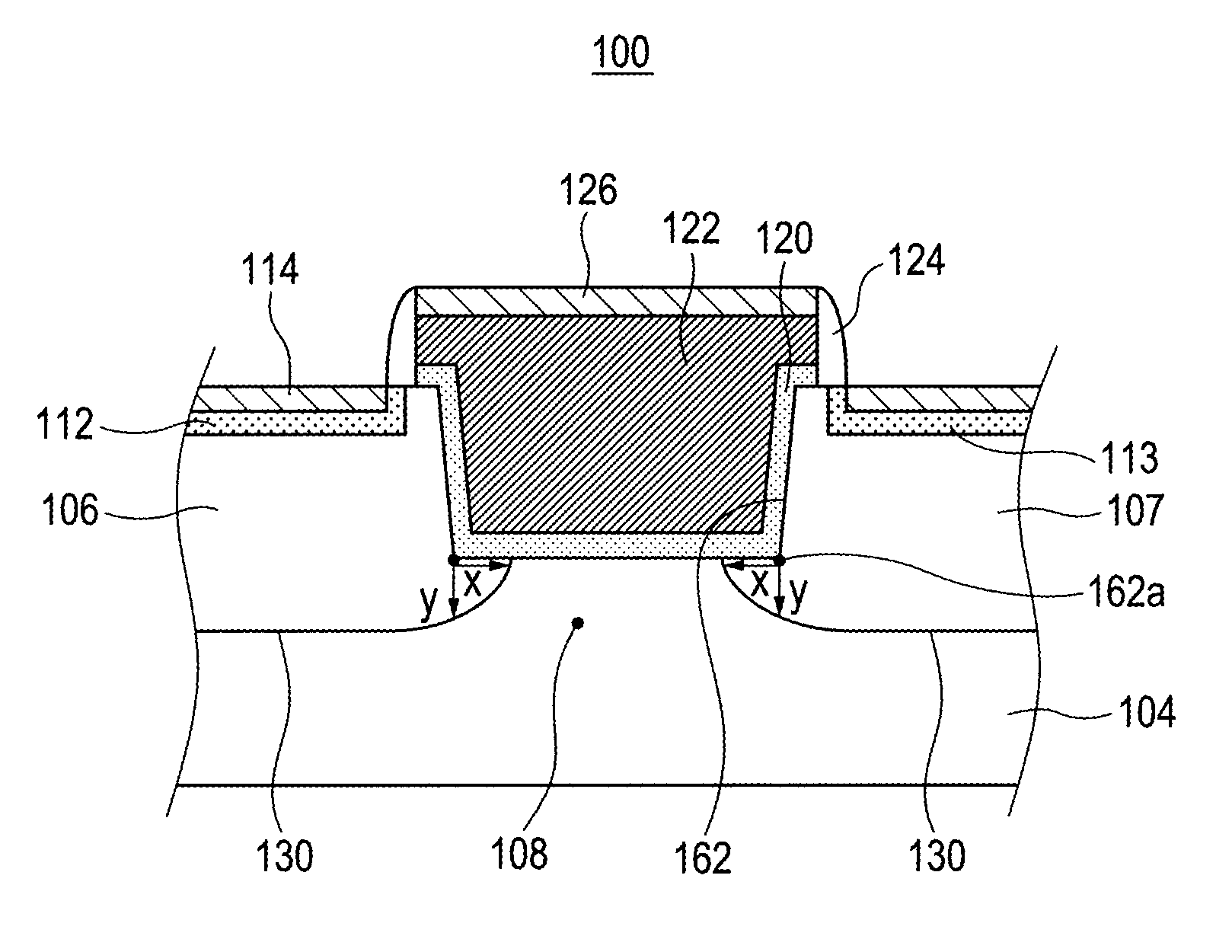
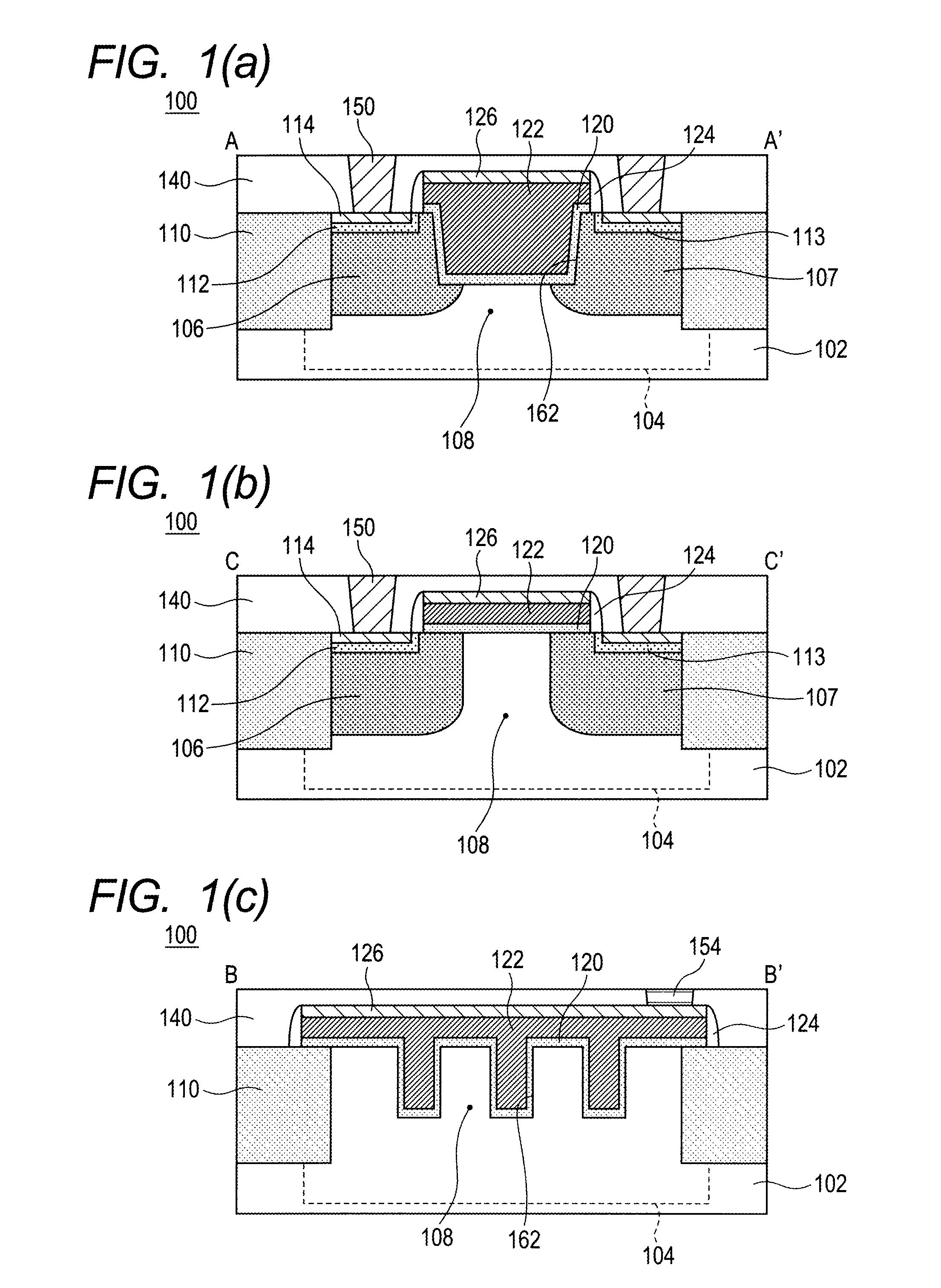
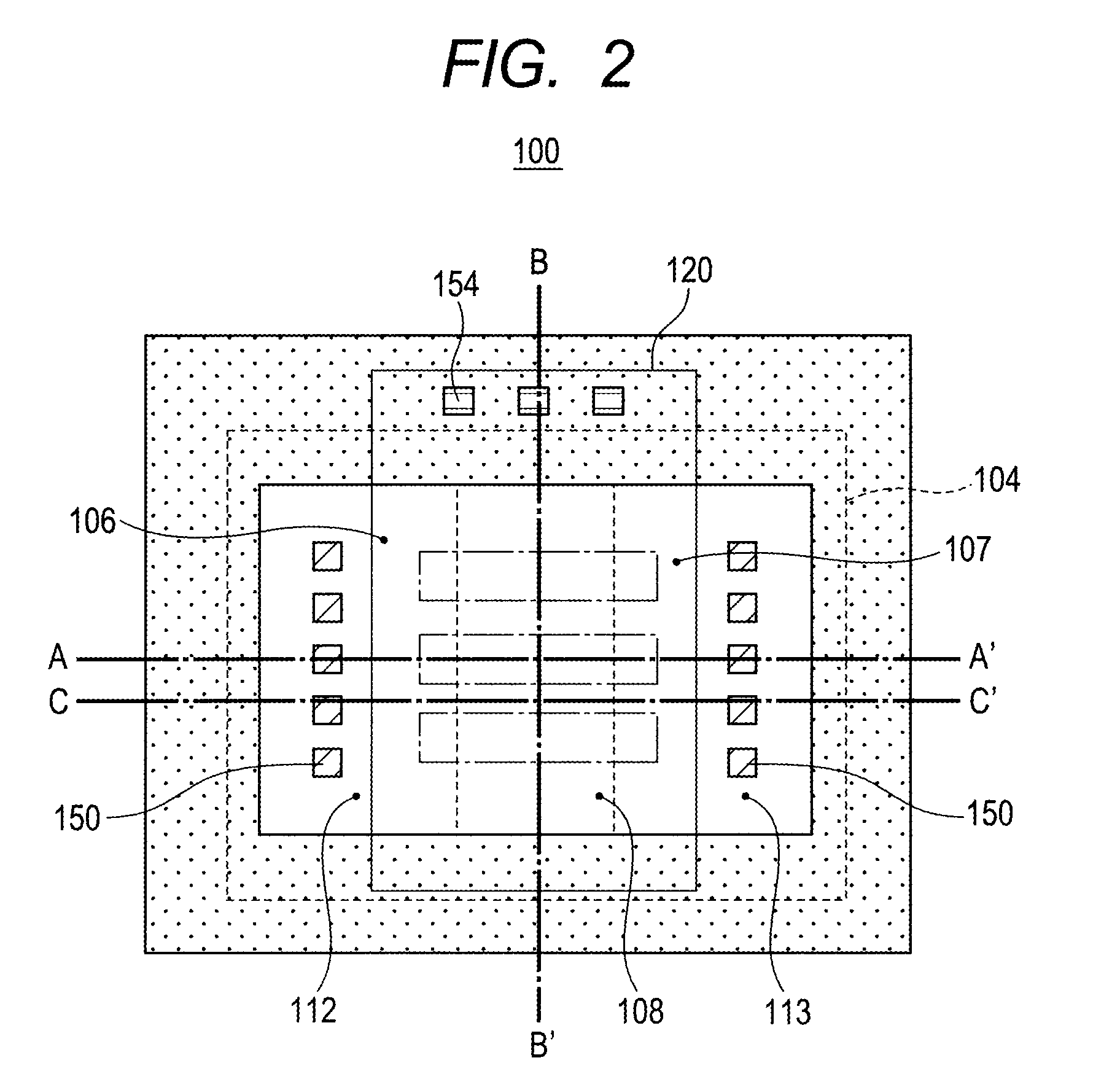
[0045]FIGS. 1(a), 1(b), and 1(c) are sectional views illustrating an embodiment of a semiconductor device according to the present invention. FIG. 2 is a plan view illustrating the embodiment of FIGS. 1(a), 1(b), and 1(c). FIG. 1(a) is a section along the line A-A′ of FIG. 2; FIG. 1(b) is a section along the line C-C′ of FIG. 2; and FIG. 1(c) is a section along the line B-B′ of FIG. 2. To ensure that the configuration is easily understandable, in FIG. 2 each region is indicated by lines alone. In the following, a case where a first conductivity type is an n-type and a second conductivity type is a p-type is described as an example. However, a reverse case may also be applied to the present invention.

[0046]A semiconductor device 100 includes a substrate 102 and transistors formed on one surface of the substrate 102. The substrate 102 can be a semiconductor substrate such as a silicon substrate. A device isolation insulating film 110 is formed on one surface of the substrate 102. The ...

second embodiment

[0089]FIGS. 13(a), 13(b), and 13(c) are sectional views illustrating an embodiment of a semiconductor device according to this embodiment. A semiconductor device 100 in this second embodiment has a similar planar configuration to that shown in FIG. 2. FIG. 13(a) is a section along the line A-A′ of FIG. 2; FIG. 13(b) is a section along the line C-C′ of FIG. 2; FIG. 13(c) is a section along the line the B-B′ of FIG. 2. In the following, a case where a first conductivity type is an n-type and a second conductivity type is a p-type is described as an example. However, a reverse case may also be applied to the present invention.

[0090]In this embodiment, the shape of the first offset region 106 and the second offset region 107 is different from that shown in FIGS. 1(a), 1(b), and 1(c). In this embodiment, the first offset region 106 and the second offset region 107 each has a depth, in the area where they contact the bottom of trench 162, greater than their depth where they make contact w...


PUM


Abstract

A trench gate transistor whose gate changes the depth thereof intermittently in the gate width direction, has a first offset region and a second offset region formed below the source and drain, respectively. The sum of length measurements of the underlying portion of the second offset region measured from the lower corner of the trench in a direction parallel to the substrate and in a direction perpendicular to the substrate is 0.1 μm or greater.

Description

CROSS-REFERENCE TO RELATED APPLICATIONS[0001]The disclosure of Japanese Patent Application No. 2009-219639 filed on Sep. 24, 2009 including the specification, drawings and abstract is incorporated herein by reference in its entirety.BACKGROUND OF THE INVENTION[0002]1. Field of the Invention[0003]The present invention relates to a semiconductor device and a manufacturing method thereof.[0004]2. Description of Related Art[0005]Techniques have been proposed for forming uneven surfaces such as trenches in the channel region of a substrate, to increase the effective channel width of a transistor without increasing in size.[0006]For example, Japanese Patent Laid-Open No. H11-103058 and Japanese Patent Laid-Open No. S51-147269 describe a semiconductor device including a trench gate structure in which trenches are formed on the substrate surface. Japanese Patent Laid-Open No. 2007-5568 describes a semiconductor device in which a plurality of projecting silicon regions are formed in the widt...

Claims


Application Information

Patent Timeline
Patent Type & Authority Patents(United States)
IPC IPC(8): H01L29/76H01L29/94H01L31/119H01L31/113H01L31/062
CPCH01L29/1037H01L29/4236H01L29/66621H01L29/66795H01L29/7834H01L29/7851H01L29/665
Inventor SANADA, KAZUHIKOKAWAGUCHI, HIROSHI
Owner RENESAS ELECTRONICS CORP
Why Eureka
Try Eureka