Light extraction product for semiconductor light emitting device and light emitting device

a technology of light emitting device and light emitting device, which is applied in the direction of lighting and heating apparatus, instruments, paper/cardboard containers, etc., can solve the problems of not being able to break the total reflection of light in the interface between the high refractive index region and the light extraction efficiency is significantly reduced, and it is not possible to extract light to the outside. , to achieve the effect of reducing color shift and glare in emitted light, improving light extraction efficiency of semiconductor ligh

Inactive Publication Date: 2015-03-19
ASAHI KASEI E-MATERIALS CORPORATION
View PDF1 Cites 40 Cited by
  • Summary
  • Abstract
  • Description
  • Claims
  • Application Information

AI Technical Summary

Benefits of technology

[0101]According to the present invention, it is possible to achieve the light extraction product for a semiconductor light emitting device for enabling light extraction efficiency from the semiconductor light emitting device to be improved, while reducing the color shift and glare in emitted light from the semiconductor light emitting device, and further enabling long-term reliability of the semiconductor light emitting device to be enhanced, and the light emitting device.

Problems solved by technology

Accordingly, it is not possible to extract the light to the outside of the semiconductor light emitting device, and light extraction efficiency significantly decreases.
However, in this method as described in Patent Document 1, it is not possible to break total reflection of light in the interface between the high refractive index region and the intermediate refractive index layer and in the interface between the intermediate refractive index layer and the low refractive index region.
Therefore, the totally reflected light maintains the waveguide mode to attenuate, and it is not expected to significantly improve light extraction efficiency.
In the method as described in Patent Document 2, since required are materials with a refractive index close to that of the high refractive index region and the waveguide mode is broken with diffracted light, light extraction efficiency is improved in only light of a critical angle or more, and it is not expected to obtain radical improvements in light extraction efficiency.
Further, glare occurs based on a diffraction color specific to diffracted light.
Further, to break the waveguide mode with diffracted light, the diffraction angle dependence for each wavelength is remarkable, and another problems also arises that an emitted light color is seen differently corresponding to an angle to visually identify i.e. so-called the color shift increases.

Method used


Image

  • Light extraction product for semiconductor light emitting device and light emitting device
  • Light extraction product for semiconductor light emitting device and light emitting device
  • Light extraction product for semiconductor light emitting device and light emitting device

Examples


embodiment 1

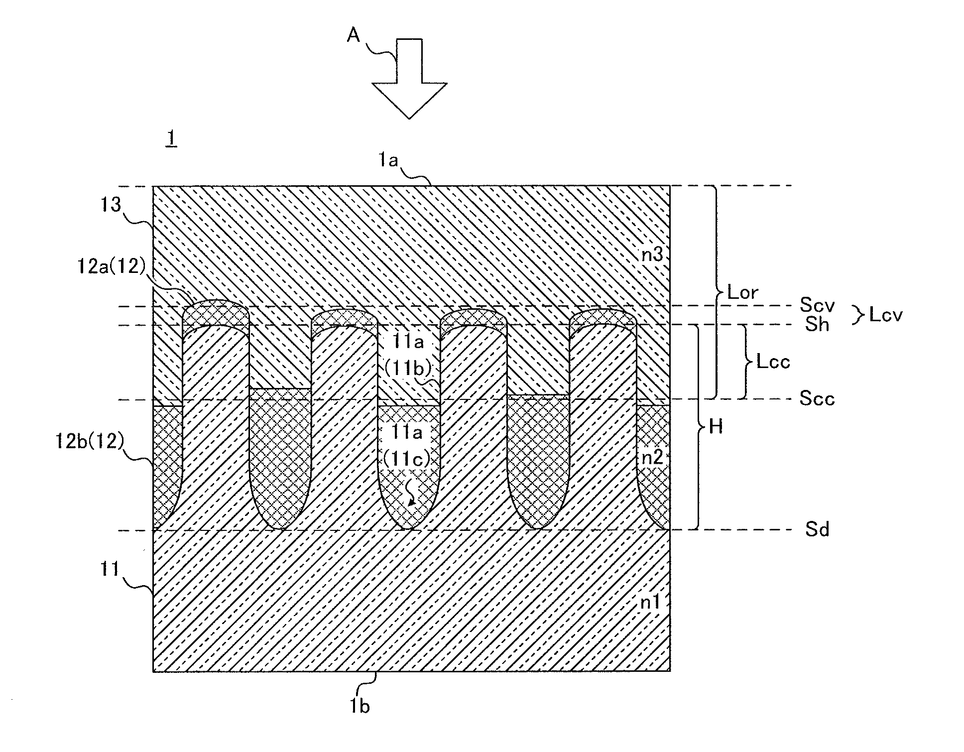
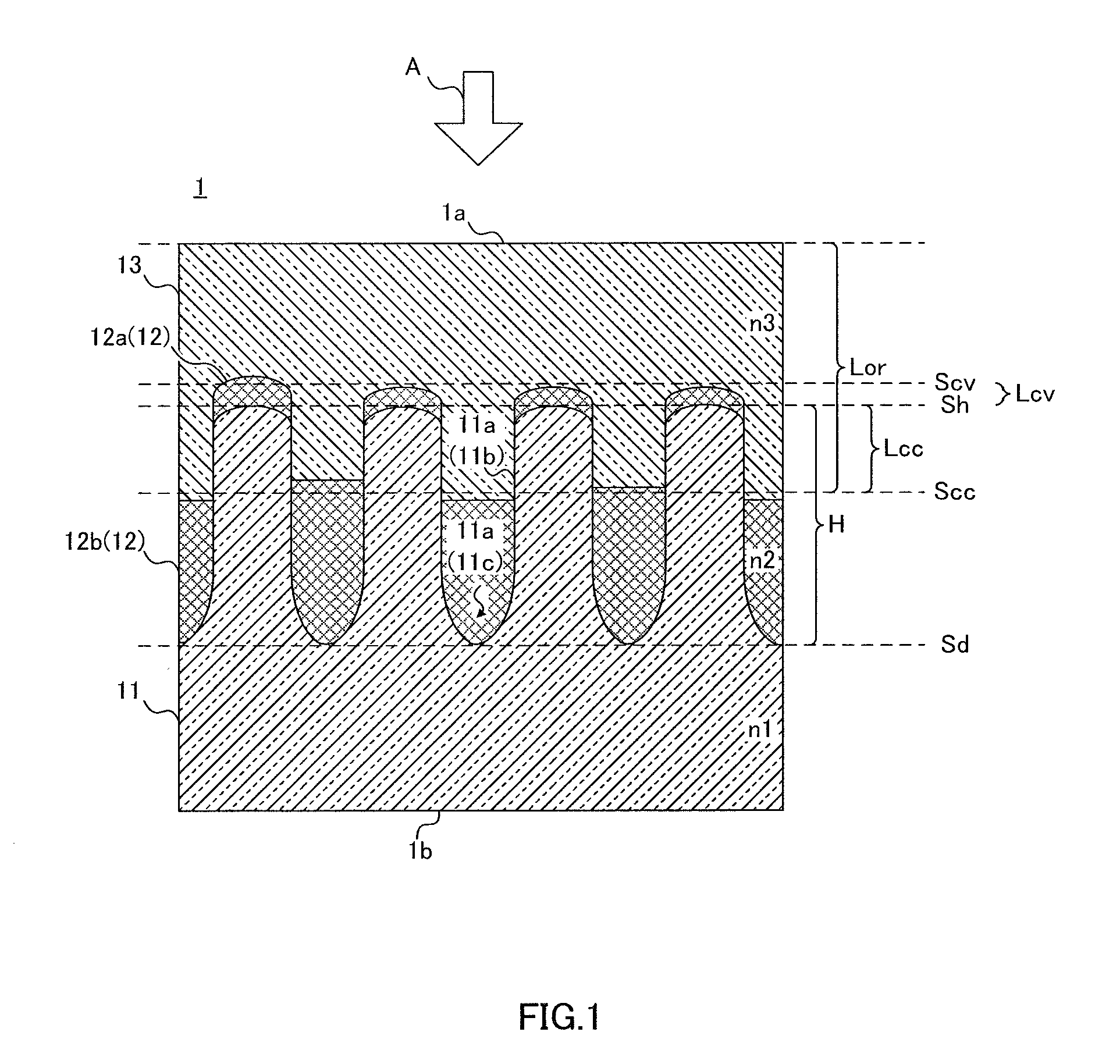
[0275]FIGS. 7 and 8 are schematic diagrams illustrating the first concavo-convex structure according to Embodiment 1. FIG. 7 is a perspective diagram illustrating a concavo-convex structure layer 101, and FIG. 8 is a top diagram of the concavo-convex structure layer shown in FIG. 7.

[0276]As shown in FIG. 7, a first concavo-convex structure 101a includes a plurality of independent convex portions 101b protruding upward in the perpendicular direction to one main surface S of the concavo-convex structure layer 101. The plurality of convex portions 101b are disposed at predetermined intervals. Portions between mutually adjacent convex portions 101b are continuously connected by a concave portion 101c dented downward in the perpendicular direction to one main surface S of the concavo-convex structure layer 101.

[0277]In the first concavo-convex structure layer 101a, the shape of the plurality of convex portions 101b is a pillar-shaped body (cone-shaped body), and the concave portion 101c ...

embodiment 2

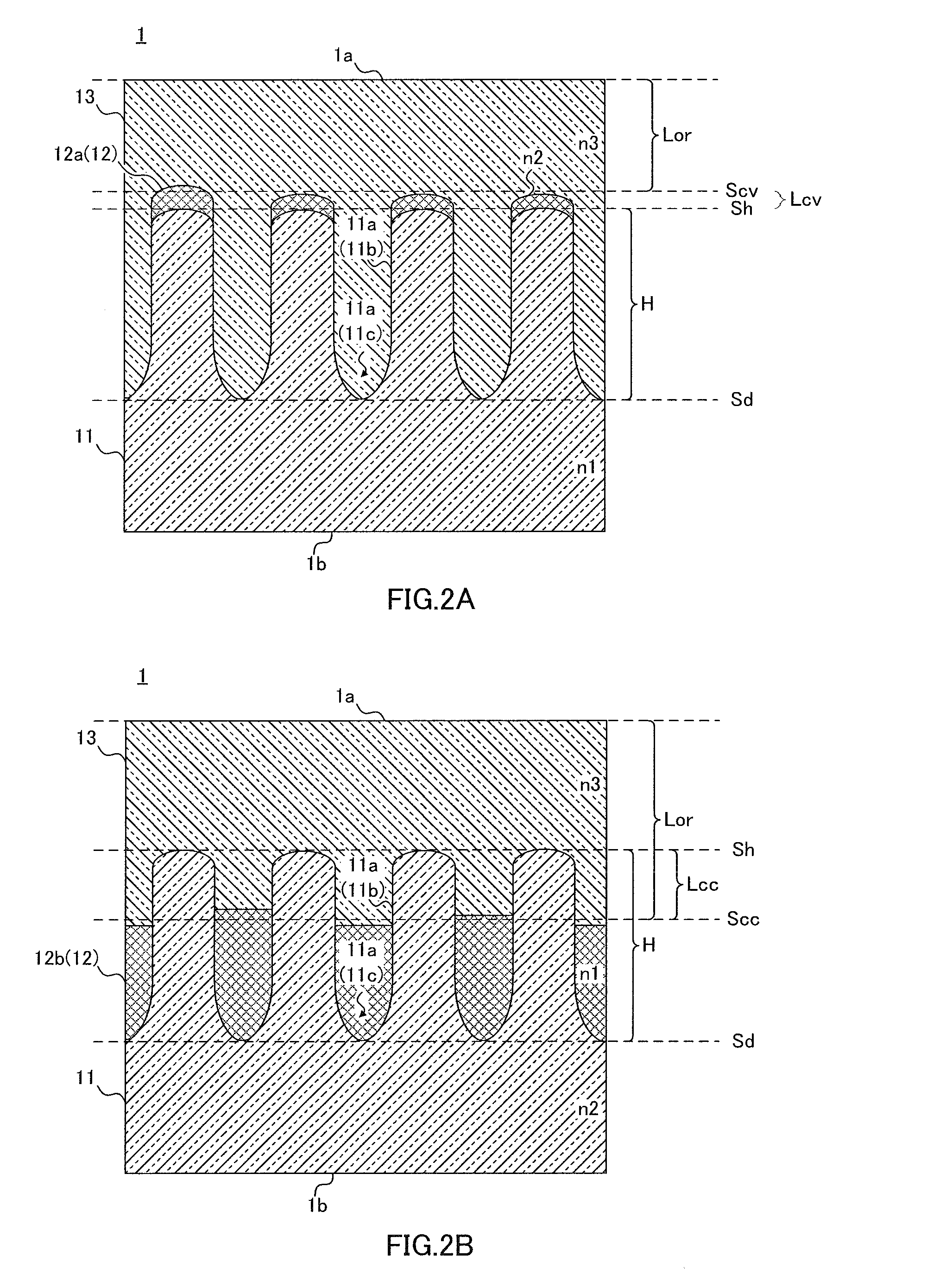
[0286]FIGS. 9 and 10 are schematic diagrams illustrating the second concavo-convex structure according to Embodiment 2. FIG. 9 is a perspective diagram illustrating a concavo-convex structure layer 111, and FIG. 10 is a top diagram of the concavo-convex structure layer 111 shown in FIG. 9.

[0287]As shown in FIG. 9, a second concavo-convex structure 111a includes a plurality of concave portions 111b dented downward in the perpendicular direction to one main surface side of the concavo-convex structure layer 111. The plurality of concave portions 111b are mutually independent and are disposed at predetermined intervals. One main surface of the concavo-convex structure layer 111 is left between mutually adjacent concave portions 111b, and forms convex portions 111c. The convex portions 111c may be mutually continuous or may be independent.

[0288]The structure includes a plurality of mutually independent concave portions 111b and convex portions 111c provided to surround the plurality of ...

embodiment 3

[0297]FIG. 11 is a schematic diagram illustrating a third concavo-convex structure according to Embodiment 3. In addition, FIG. 11 schematically shows a state in which a concavo-convex structure layer 121 is viewed from the upper surface.

[0298]As shown in FIG. 11, a third concavo-convex structure 121a includes a plurality of mutually parallel palisade bodies (convex portions) 121b extending along the first direction D1 belonging to the inside of the main surface of the concavo-convex structure layer 121. Each palisade body 121b is provided to protrude perpendicularly upward from the main surface of the concavo-convex structure layer 121, and has a predetermined thickness (width) in the second direction D2 orthogonal to the first direction D1. Further, one main surface of the concavo-convex structure layer 121 is left between respective palisade bodies 121b, and forms concave portions 121c provided between respective palisade bodies 121b.

[0299]In other words, in the case where the l...


PUM

PropertyMeasurementUnit
refractive indexaaaaaaaaaa
diameteraaaaaaaaaa
diameteraaaaaaaaaa

Abstract

A light extraction product (1) for a semiconductor light emitting device is provided with a concavo-convex structure layer (11), provided with a concavo-convex structure (11a) on a surface thereof, having a first refractive index (n1) and a light extraction layer (12), provided on the convex portion of the concavo-convex structure (11a), having a second refractive index (n2), where in a first light extraction layer (12a) a distance Lcv between an average position Sh of tops of the convex-portions and a convex-portion upper interface average position Scv of the first light extraction layer (12a) meets equation (1) 10 nm≦Lcv≦5000 nm, in the concavo-convex structure (11a) a convex-portion average height H meets equation (2) 10 nm≦H≦5000 nm, an average pitch P meets equation (3) 50 nm≦P≦5000 nm, and the distance Lcv and the convex-portion average height H meet equation (4) 50 nm≦Lcv+H≦6000 nm. It is possible to improve light extraction efficiency from the semiconductor light emitting device using the light extraction product (1), and further to enhance long-term reliability of the semiconductor light emitting device.

Description

TECHNICAL FIELD[0001]The present invention relates to a light extraction product for semiconductor light emitting device and light emitting device, and for example, to a light extraction product for semiconductor light emitting device suitably used in a semiconductor light emitting device such as an organic EL device and LED, and light emitting device.BACKGROUND ART[0002]In recent years, in order to improve luminous efficiency in a semiconductor light emitting device such as an organic EL device, fluorescent product and LED, improvements have been studied in light extraction efficiency from the semiconductor light emitting device. Such a semiconductor light emitting device has a configuration that a high refractive index region is sandwiched between low refractive index regions and that a light emitting portion is included inside the high refractive index region. Therefore, emitted light emitted in the light emitting portion becomes a waveguide mode that the light is guided inside t...

Claims


Application Information

Patent Timeline
Patent Type & Authority Applications(United States)
IPC IPC(8): H01L51/52B32B37/00B32B38/10G02B5/18B32B37/24
CPCH01L51/5275G02B5/18G02B5/1847B32B2551/08B32B38/10B32B37/025B32B2037/243B32B37/24G02B1/118G02B5/0294G02B5/1809G02B5/1814H01L33/58H01L2933/0058H01L2933/0091H10K50/858H10K2101/00H10K2102/351Y10T156/10G02B1/16H10K2102/331H10K50/85G02F1/133502
Inventor YAMAGUCHI, FUJITOKOIKE, JUNTAKAGIWA, AYA
Owner ASAHI KASEI E-MATERIALS CORPORATION
Why Eureka
Try Eureka