Vertically packaged MOSFET and IC power devices as integrated module using 3D interconnected laminates

a technology of interconnected laminates and integrated modules, which is applied in the direction of semiconductor devices, semiconductor/solid-state device details, electrical apparatus, etc., can solve the problems of thermal mismatch between the metal lines of the leadframe and the printed circuit board, the failure rate of solder joints is higher, and the mechanical structure is conventional, so as to achieve convenient stacking

Active Publication Date: 2007-04-19
ALPHA & OMEGA SEMICON LTD
View PDF30 Cites 37 Cited by
  • Summary
  • Abstract
  • Description
  • Claims
  • Application Information

AI Technical Summary

Benefits of technology

[0014] It is therefore an object of the present invention to make it possible to package MOSFET device together with power IC and other passive components like capacitors and resistors into 3D integrated module stack form with the help of an improved configuration for packaging a vertical semiconductor device such as a MOSFET device by forming interconnecting traces in laminated layers. The laminated layers are composed of materials that have similar coefficient of thermal expansion as that of printed circuit board and reduces thermal mismatch problems.
[0015] It is another aspect of this invention that the laminated multi-layer carrier such as a PCB or flexible board formed with interconnecting traces improves the yield of packaging processes and produces packages with improved long term reliability. The packaging configuration further provides more flexibly adjustable die size without being limited by specially processed die-attaching carriers formed with special cavity or shapes and sizes with extended edges as that shown above. With commonly available PCB technologies now applied in semiconductor packaging processes, another aspect of this invention is that the configuration disclosed in this invention can be conveniently implemented as a surface mount technology (SMT) package. Because of the flexibility and adaptability of the configuration, the packaging configuration of the present invention can be a convenient replacement of conventional lead frame type packages such as packaging families of SO, TSSOP and TO. Another aspect of this invention is the improvement that the process has improved sight to the solder joint area thus significantly improves the convenience and manufacturability of the packaging processes.
[0016] Another aspect of the present invention is to provide an improved configuration for packaging a MOSFET device with available multiple chips packaging on the same layer thus resolve the above-discussed limitations and difficulties of the conventional packaging configurations.
[0019] This invention further discloses a method for configuring an electronic package for containing at least a top packaging module vertically stacked on a bottom packaging module. The method includes a step of fabricating a multi-layered laminated board with a standard printed-circuit board process for providing via connectors and connecting traces for packaging a semiconductor in each of the top and bottom packaging modules. The method further includes a step of fabricating and configuring the top and bottom packaging module as a surface mountable modules for conveniently stacking and mounting to prearranged electrical contacts without using a leadframe. In a preferred embodiment, the method further includes a step of fabricating and configuring at least one of the top and bottom packaging module as a multi-chip module (MCM) containing at least two semiconductor chips. In another preferred embodiment, the method further includes a step of fabricating and configuring a ball grid array (BGA) on a bottom surface of at least one of the top and bottom packaging modules for surface mounting onto the prearranged electrical contacts. In another preferred embodiment, the method further includes a step of fabricating and configuring a solder bump array on a bottom surface of at least one of the top and bottom packaging modules for surface mounting onto the prearranged electrical contacts.

Problems solved by technology

Packaging technologies as currently available and the configurations commonly implemented to package the vertical semiconductor devices, e.g., the power MOSFET devices, still face a problem that a leadframe or ceramic substrate is commonly used.
There is a thermal mismatch between the metal lines of the leadframe and the printed circuit board (PCB) supporting the electronic device and the leadframe.
Due to the thermal mismatch, there is a higher failure rate of solder joints.
Furthermore, the conventional mechanical structure has several drawbacks such as the unevenness of the die-lead frame system, the limited die size due to the lead frame limitation, and limitation of stress absorption during board level mounting.
Current packaging technologies further has another limitation where there is an assembly acceptance difficulty that often causes higher assembly cost and makes it difficult to replace the conventional high volume packages, such as SO, TO and TSSOP package families to reduce the packaging costs.
Such difficulty is caused by the fact that these packages cannot be completely packaged by either a lead frame type packaging technology or a regular surface mount assembly technology.
These packages further introduce another difficulty in the board level during the pre-assembly and testing processes due to the operations which are conducted under a sightless condition of the solder joint area between package and PCB.
The use of lead frame in these packaging technologies further limits the package to a single die configuration because of the fact that the leadframes do not provide flexibilities to be adaptable to the multiple-chip configuration either as a single module or as an assembly comprised of several modules.
Even that this package has the benefits of reducing the package resistance and offers much improved thermal performance, the package has higher production cost due to the requirement to specially manufacture the carrier 106 with specially shaped cavity.
Furthermore, due to the geometric shape of the carrier 106, the package as disclosed by Joshi still lacks the flexibility to adapt to different packaging configurations including the multiple-chip module (MCM) configuration.
However, since the at least one or two layers of this multi-layered substrate is composed of metal, the problem of thermal expansion mismatches between the metal layer and the printed circuit board for supporting the package would still cause thermal stresses.
The package is still limited by a reliability problem when operated under thermally challenging environment.
However, it only applies to semiconductor chips where electrical contacts are formed on the same surface.
However, the ATAB carriers are too thin to maintain its shape, stiffeners need to be used to increase the complexity and package size.
Furthermore the disclosed packaging technique is only applicable to package semiconductor chips where all electrical contacts are on the same surface (planar device).
Therefore, the above patented disclosures do not provide a practical solution to overcome the limitations and difficulties as now encountered by a person of ordinary skill in the art of semiconductor device packaging design and manufactures.
Furthermore, none of above disclosures can be used for 3D packaging for vertical power MOSFET device and power IC module.

Method used


Image

  • Vertically packaged MOSFET and IC power devices as integrated module using 3D interconnected laminates
  • Vertically packaged MOSFET and IC power devices as integrated module using 3D interconnected laminates
  • Vertically packaged MOSFET and IC power devices as integrated module using 3D interconnected laminates

Examples


Embodiment Construction

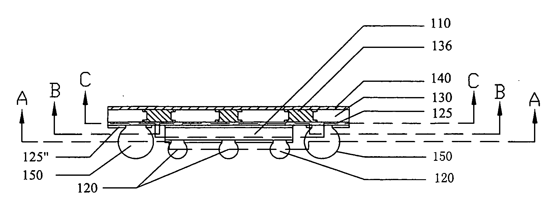
[0026] Referring to FIGS. 2A and 2B for a side cross sectional view and a bottom view of a new MOSFET package 100 of this invention. The MOSFET package 100 includes a MOSFET semiconductor chip 110 that has a plurality of solder bumps 120 and 121. The solder bumps 120 and 121 are in electrical contact to the source pad and gate pad disposed on the top surface of the MOSFET chip 110. A plurality of copper traces 125 is connected to the drain contact disposed on the bottom surface of the MOSFET chip 110. A copper plate 125′ is electroplated to a laminated board, e.g., a printed circuit board (PCB) 130, that has a plurality of via connector filled with copper 135 therein to connect to the top surface. A top copper plate 140 is further electroplated to the top surface of the laminated board, e.g., the PCB 130. A ball grid array (BGA) that includes a plurality of solder balls 150 is disposed on the bottom surface of the PCB 130. The balls 150 of the BGA are in electric contact with the co...


PUM


Abstract

An electronic package for containing at least a top packaging module vertically stacked on a bottom packaging module. Each of the packaging modules includes a semiconductor chip packaged and connected by via connectors and connectors disposed on a laminated board fabricated with a standard printed-circuit board process wherein the top and bottom packaging module further configured as a surface mountable modules for conveniently stacking and mounting to prearranged electrical contacts without using a leadframe. At least one of the top and bottom packaging modules is a multi-chip module (MCM) containing at least two semiconductor chips. At least one of the top and bottom packaging modules includes a ball grid array (BGA) for surface mounting onto the prearranged electrical contacts. At least one of the top and bottom packaging modules includes a plurality of solder bumps on one of the semiconductor chips for surface mounting onto the prearranged electrical contacts. The laminated board of the bottom packaging modules further has a thermal expansion coefficient substantially the same as a printed circuit board (PCB) whereby a surface mount onto the PCB is less impacted by a temperature change

Description

[0001] This is a Continuous-In-Part (CIP) Application of a previously filed co-pending Application with Ser. No. 11 / 220,759 filed on Sep. 6, 2005 by identical common inventors of this Application. Applications Ser. No. 11 / 220,759 is hereby incorporated by reference in this Patent Application.BACKGROUND OF THE INVENTION [0002] 1. Field of the Invention [0003] The invention relates generally to the process and configuration for packaging integrated circuits such as power MOSFETs and other types of integrated circuits, such as power IC. More particularly, this invention relates to a novel and improved method and configuration for simplifying and streamlining the MOSFET and IC device package processes as highly integrated module to achieve lower production cost, higher packaging throughput and packages with improved reliability. [0004] 2. Description of the Prior Art [0005] Packaging technologies as currently available and the configurations commonly implemented to package the vertical ...

Claims


Application Information

Patent Timeline
Patent Type & Authority Applications(United States)
IPC IPC(8): H01L23/02
CPCH01L23/3677H01L23/49816H01L23/49844H01L23/5389H01L2224/16225H01L2224/48091H01L2224/48227H01L2924/01078H01L2924/01079H01L2924/15311H01L2924/15331H01L2924/19041H01L2924/30107H01L2924/00014H01L24/48H01L2924/13091H01L2224/32225H01L2224/73253H01L2224/73265H01L2924/00012H01L2924/00H01L2924/10253H01L24/73H01L2924/14H01L2924/181H01L2224/45099H01L2224/45015H01L2924/207
Inventor SUN, MINGHO, YUEH SE
Owner ALPHA & OMEGA SEMICON LTD
Why Eureka
Try Eureka