Nano metal particles based tunneling field effect transistor and nano-switch
a tunneling field effect transistor and metal particle technology, applied in the direction of diodes, semiconductor devices, electrical apparatus, etc., can solve the problems of limited scaling down device size, high electric field at the interface, and only minimal loss of energy for devices, so as to minimize the energy consumption of electronic devices, reduce the loss of energy, and achieve the effect of high switching speed
- Summary
- Abstract
- Description
- Claims
- Application Information
AI Technical Summary
Benefits of technology
Problems solved by technology
Method used
Image


Examples
Embodiment Construction
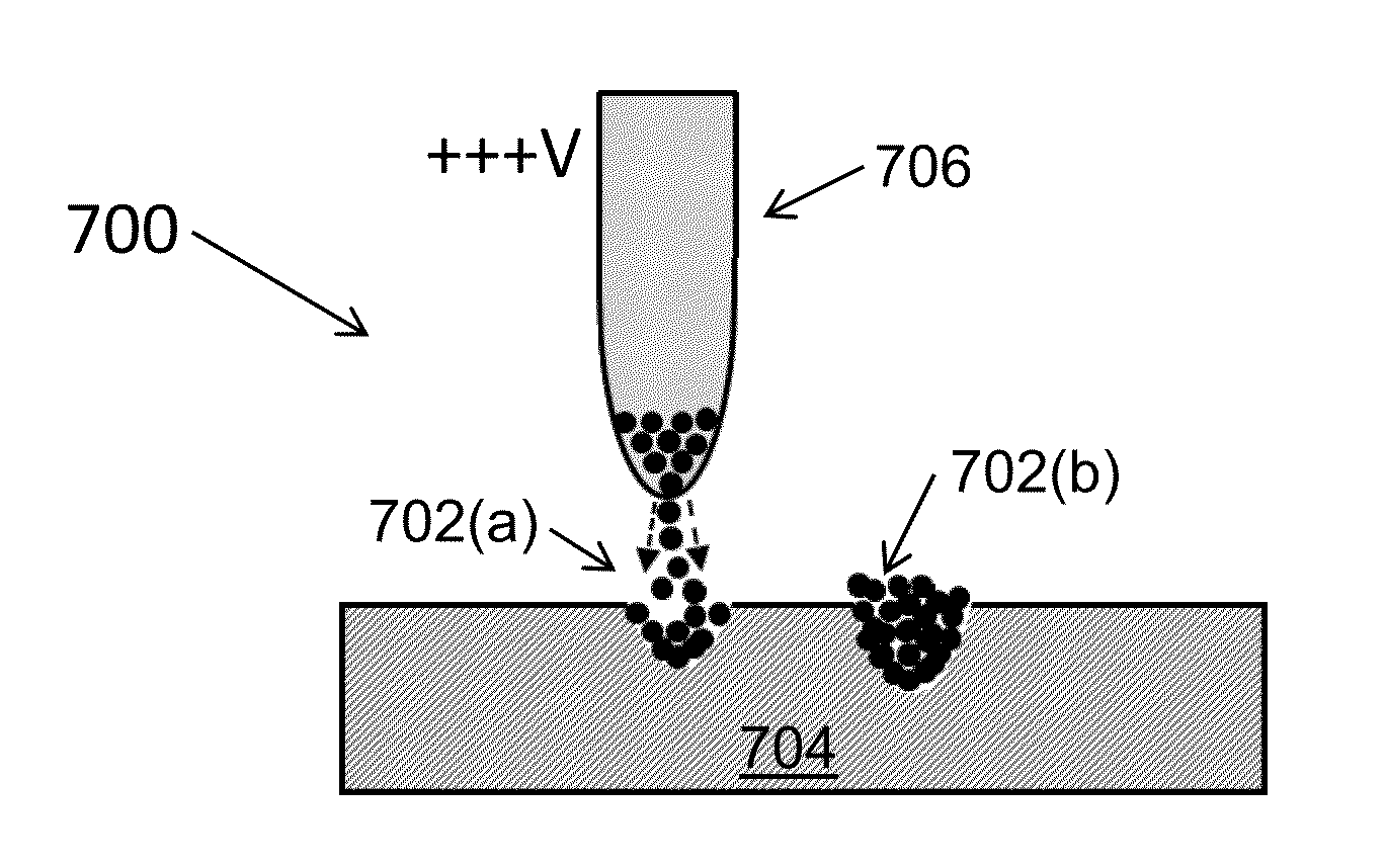
[0039]The present inventor's approach to fabricating a nano TEFT utilizes the properties of nano metal semiconductor junctions by implanting nano clusters or nano particles of metal atoms in the surface of a single n-doped silicon (Si) substrate. Instead of having the source, bulk and drain with alternating dopants, in the present invention the source and drain are made of nano clusters of metal atoms, implanted into the doped semiconductor substrate. In the present invention, the source will be about 1-2 nm in average radius and the drain may be of the same size or slightly larger, e.g., about 3-4 nm in radius.
[0040]FIG. 1(a) schematically depicts an embodiment of a nano metal tunneling FET 100 in accordance with an embodiment of the present invention. As shown in FIG. 1, the nano metal TFET 100 includes a semiconductor substrate 102, e.g., a moderate or low n-doped silicon semiconductor, or other semiconductors having similar energy band structure, over which has been deposited a ...
PUM
| Property | Measurement | Unit |
|---|---|---|
| average radius | aaaaa | aaaaa |
| distance | aaaaa | aaaaa |
| size | aaaaa | aaaaa |
Abstract
Description
Claims
Application Information